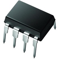
PIC12LCE673-04I/P Microchip Technology, PIC12LCE673-04I/P Datasheet - Page 37

PIC12LCE673-04I/P
Manufacturer Part Number
PIC12LCE673-04I/P
Description
IC MCU OTP 1KX14 LV A/D EE 8DIP
Manufacturer
Microchip Technology
Series
PIC® 12Cr
Specifications of PIC12LCE673-04I/P
Core Processor
PIC
Core Size
8-Bit
Speed
4MHz
Peripherals
POR, WDT
Number Of I /o
5
Program Memory Size
1.75KB (1K x 14)
Program Memory Type
OTP
Eeprom Size
16 x 8
Ram Size
128 x 8
Voltage - Supply (vcc/vdd)
2.5 V ~ 5.5 V
Data Converters
A/D 4x8b
Oscillator Type
Internal
Operating Temperature
-40°C ~ 85°C
Package / Case
8-DIP (0.300", 7.62mm)
Processor Series
PIC12LC
Core
PIC
Data Bus Width
8 bit
Data Ram Size
128 B
Maximum Clock Frequency
4 MHz
Number Of Programmable I/os
5
Number Of Timers
8
Operating Supply Voltage
2.5 V to 5.5 V
Maximum Operating Temperature
+ 85 C
Mounting Style
Through Hole
3rd Party Development Tools
52715-96, 52716-328, 52717-734
Development Tools By Supplier
ICE2000
Minimum Operating Temperature
- 40 C
On-chip Adc
8
Data Rom Size
128 B
Height
3.3 mm
Length
9.27 mm
Supply Voltage (max)
5.5 V
Supply Voltage (min)
2.5 V
Width
6.35 mm
Lead Free Status / RoHS Status
Lead free / RoHS Compliant
Connectivity
-
Lead Free Status / Rohs Status
Details
Available stocks
Company
Part Number
Manufacturer
Quantity
Price
Part Number:
PIC12LCE673-04I/P
Manufacturer:
MICROCHIP/微芯
Quantity:
20 000
6.5
Read operations are initiated in the same way as write
operations with the exception that the R/W bit of the
EEPROM address is set to one. There are three basic
types of read operations; current address read, random
read and sequential read.
6.5.1
The EEPROM contains an address counter that main-
tains the address of the last word accessed, internally
incremented by one. Therefore, if the previous read
access was to address n, the next current address read
operation would access data from address n + 1. Upon
receipt of the EEPROM address with the R/W bit set to
one, the EEPROM issues an acknowledge and trans-
mits the 8-bit data word. The processor will not
acknowledge the transfer, but does generate a stop
condition and the EEPROM discontinues transmission
(Figure 6-8).
6.5.2
Random read operations allow the processor to access
any memory location in a random manner. To perform
this type of read operation, first the word address must
be set. This is done by sending the word address to the
EEPROM as part of a write operation. After the word
FIGURE 6-8:
FIGURE 6-9:
FIGURE 6-10: SEQUENTIAL READ
1999 Microchip Technology Inc.
SDA LINE
ACTIVITY
Read Operations
CURRENT ADDRESS READ
RANDOM READ
X = Don’t Care Bit
SDA LINE
ACTIVITY
CURRENT ADDRESS READ
RANDOM READ
CONTROL
BYTE
S
T
A
R
T
S 1
A
C
K
0
CONTROL
SDA LINE
ACTIVITY
1
X = Don’t Care Bit
BYTE
0 X X X 0
DATA n
A
C
K
X X X X
A
C
K
ADDRESS (n)
S
T
A
R
T
S
WORD
1
DATA n + 1
0
CONTROL
1
BYTE
0 X X X 1
address is sent, the processor generates a start condi-
tion following the acknowledge. This terminates the
write operation, but not before the internal address
pointer is set. Then the processor issues the control
byte again, but with the R/W bit set to a one. The
EEPROM will then issue an acknowledge and trans-
mits the 8-bit data word. The processor will not
acknowledge the transfer, but does generate a stop
condition and the EEPROM discontinues transmission
(Figure 6-9). After this command, the internal address
counter will point to the address location following the
one that was just read.
6.5.3
Sequential reads are initiated in the same way as a ran-
dom read, except that after the device transmits the first
data byte, the processor issues an acknowledge as
opposed to a stop condition in a random read. This
directs the EEPROM to transmit the next sequentially
addressed 8-bit word (Figure 6-10).
To provide sequential reads, the EEPROM contains an
internal address pointer, which is incremented by one
at the completion of each read operation. This address
pointer allows the entire memory contents to be serially
read during one operation.
A
C
K
S
T
A
R
T
S 1
A
C
K
A
C
K
0
CONTROL
DATA n + 2
1
SEQUENTIAL READ
BYTE
0 X X X 1
DATA
A
C
K
A
C
K
N
O
A
C
K
S
T
O
P
P
PIC12C67X
DATA (n)
DATA n + X
DS30561B-page 37
N
O
C
A
K
S
T
O
P
P
N
O
A
C
K
S
T
O
P
P


