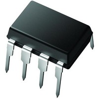
PIC12LCE673-04I/P Microchip Technology, PIC12LCE673-04I/P Datasheet - Page 45

PIC12LCE673-04I/P
Manufacturer Part Number
PIC12LCE673-04I/P
Description
IC MCU OTP 1KX14 LV A/D EE 8DIP
Manufacturer
Microchip Technology
Series
PIC® 12Cr
Specifications of PIC12LCE673-04I/P
Core Processor
PIC
Core Size
8-Bit
Speed
4MHz
Peripherals
POR, WDT
Number Of I /o
5
Program Memory Size
1.75KB (1K x 14)
Program Memory Type
OTP
Eeprom Size
16 x 8
Ram Size
128 x 8
Voltage - Supply (vcc/vdd)
2.5 V ~ 5.5 V
Data Converters
A/D 4x8b
Oscillator Type
Internal
Operating Temperature
-40°C ~ 85°C
Package / Case
8-DIP (0.300", 7.62mm)
Processor Series
PIC12LC
Core
PIC
Data Bus Width
8 bit
Data Ram Size
128 B
Maximum Clock Frequency
4 MHz
Number Of Programmable I/os
5
Number Of Timers
8
Operating Supply Voltage
2.5 V to 5.5 V
Maximum Operating Temperature
+ 85 C
Mounting Style
Through Hole
3rd Party Development Tools
52715-96, 52716-328, 52717-734
Development Tools By Supplier
ICE2000
Minimum Operating Temperature
- 40 C
On-chip Adc
8
Data Rom Size
128 B
Height
3.3 mm
Length
9.27 mm
Supply Voltage (max)
5.5 V
Supply Voltage (min)
2.5 V
Width
6.35 mm
Lead Free Status / RoHS Status
Lead free / RoHS Compliant
Connectivity
-
Lead Free Status / Rohs Status
Details
Available stocks
Company
Part Number
Manufacturer
Quantity
Price
Part Number:
PIC12LCE673-04I/P
Manufacturer:
MICROCHIP/微芯
Quantity:
20 000
8.0
The Analog-To-Digital (A/D) converter module has four
analog inputs.
The A/D allows conversion of an analog input signal to
a corresponding 8-bit digital number (refer to Applica-
tion Note AN546 for use of A/D Converter). The output
of the sample and hold is the input into the converter,
which generates the result via successive approxima-
tion. The analog reference voltage is software select-
able to either the device’s positive supply voltage (V
or the voltage level on the GP1/AN1/V
converter has a unique feature of being able to operate
while the device is in SLEEP mode.
The A/D module has three registers. These registers
are:
REGISTER 8-1:
1999 Microchip Technology Inc.
bit7
bit 7-6: ADCS<1:0>: A/D Conversion Clock Select bits
bit 5:
bit 4-3: CHS<1:0>: Analog Channel Select bits
bit 2:
bit 1:
bit 0:
ADCS1 ADCS0 reserved
R/W-0
• A/D Result Register (ADRES)
• A/D Control Register 0 (ADCON0)
• A/D Control Register 1 (ADCON1)
ANALOG-TO-DIGITAL
CONVERTER (A/D) MODULE
00 = F
01 = F
10 = F
11 = F
Reserved
00 = channel 0, (GP0/AN0)
01 = channel 1, (GP1/AN1)
10 = channel 2, (GP2/AN2)
11 = channel 3, (GP4/AN3)
GO/DONE: A/D Conversion Status bit
If ADON = 1
1 = A/D conversion in progress (setting this bit starts the A/D conversion)
0 = A/D conversion not in progress (this bit is automatically cleared by hardware when the A/D conversion
is complete)
Reserved
ADON: A/D on bit
1 = A/D converter module is operating
0 = A/D converter module is shut off and consumes no operating current
R/W-0
OSC
OSC
OSC
RC
(clock derived from an RC oscillation)
/2
/8
/32
ADCON0 REGISTER (ADDRESS 1Fh)
R/W-0
R/W-0
CHS1
REF
pin. The A/D
R/W-0
CHS0
DD
GO/DONE reserved
)
R/W-0
The ADCON0 Register, shown in Figure 8-1, controls
the operation of the A/D module. The ADCON1 Regis-
ter, shown in Figure 8-2, configures the functions of the
port pins. The port pins can be configured as analog
inputs (GP1 can also be a voltage reference) or as dig-
ital I/O.
Note 1: If the port pins are configured as analog
R/W-0
2: Changing ADCON1 Register can cause
inputs (reset condition), reading the port
(MOVF GPIO,W) results in reading '0's.
the GPIF and INTF flags to be set in the
INTCON Register.
should be disabled prior to modifying
ADCON1.
ADON
R/W-0
bit0
PIC12C67X
R = Readable bit
W = Writable bit
U = Unimplemented bit,
- n = Value at POR reset
read as ‘0’
These interrupts
DS30561B-page 45


