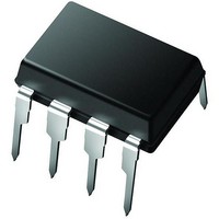
PIC12LCE673-04I/P Microchip Technology, PIC12LCE673-04I/P Datasheet - Page 16

PIC12LCE673-04I/P
Manufacturer Part Number
PIC12LCE673-04I/P
Description
IC MCU OTP 1KX14 LV A/D EE 8DIP
Manufacturer
Microchip Technology
Series
PIC® 12Cr
Specifications of PIC12LCE673-04I/P
Core Processor
PIC
Core Size
8-Bit
Speed
4MHz
Peripherals
POR, WDT
Number Of I /o
5
Program Memory Size
1.75KB (1K x 14)
Program Memory Type
OTP
Eeprom Size
16 x 8
Ram Size
128 x 8
Voltage - Supply (vcc/vdd)
2.5 V ~ 5.5 V
Data Converters
A/D 4x8b
Oscillator Type
Internal
Operating Temperature
-40°C ~ 85°C
Package / Case
8-DIP (0.300", 7.62mm)
Processor Series
PIC12LC
Core
PIC
Data Bus Width
8 bit
Data Ram Size
128 B
Maximum Clock Frequency
4 MHz
Number Of Programmable I/os
5
Number Of Timers
8
Operating Supply Voltage
2.5 V to 5.5 V
Maximum Operating Temperature
+ 85 C
Mounting Style
Through Hole
3rd Party Development Tools
52715-96, 52716-328, 52717-734
Development Tools By Supplier
ICE2000
Minimum Operating Temperature
- 40 C
On-chip Adc
8
Data Rom Size
128 B
Height
3.3 mm
Length
9.27 mm
Supply Voltage (max)
5.5 V
Supply Voltage (min)
2.5 V
Width
6.35 mm
Lead Free Status / RoHS Status
Lead free / RoHS Compliant
Connectivity
-
Lead Free Status / Rohs Status
Details
Available stocks
Company
Part Number
Manufacturer
Quantity
Price
Part Number:
PIC12LCE673-04I/P
Manufacturer:
MICROCHIP/微芯
Quantity:
20 000
PIC12C67X
4.2.2.2
The OPTION Register is a readable and writable regis-
ter, which contains various control bits to configure the
TMR0/WDT prescaler, the External INT Interrupt,
TMR0 and the weak pull-ups on GPIO.
REGISTER 4-2:
DS30561B-page 16
bit7
bit 7:
bit 6:
bit 5:
bit 4:
bit 3:
bit 2-0: PS<2:0>: Prescaler Rate Select bits
GPPU
R/W-1
OPTION REGISTER
GPPU: Weak Pull-up Enable
1 = Weak pull-ups disabled
0 = Weak pull-ups enabled (GP0, GP1, GP3)
INTEDG: Interrupt Edge
1 = Interrupt on rising edge of GP2/T0CKI/AN2/INT pin
0 = Interrupt on falling edge of GP2/T0CKI/AN2/INT pin
T0CS: TMR0 Clock Source Select bit
1 = Transition on GP2/T0CKI/AN2/INT pin
0 = Internal instruction cycle clock (CLKOUT)
T0SE: TMR0 Source Edge Select bit
1 = Increment on high-to-low transition on GP2/T0CKI/AN2/INT pin
0 = Increment on low-to-high transition on GP2/T0CKI/AN2/INT pin
PSA: Prescaler Assignment bit
1 = Prescaler is assigned to the WDT
0 = Prescaler is assigned to the Timer0 module
INTEDG
Bit Value
R/W-1
000
001
010
011
100
101
110
111
OPTION REGISTER (ADDRESS 81h)
R/W-1
T0CS
TMR0 Rate
1 : 2
1 : 4
1 : 8
1 : 16
1 : 32
1 : 64
1 : 128
1 : 256
R/W-1
T0SE
WDT Rate
1 : 1
1 : 2
1 : 4
1 : 8
1 : 16
1 : 32
1 : 64
1 : 128
R/W-1
PSA
R/W-1
PS2
R/W-1
Note:
PS1
To achieve a 1:1 prescaler assignment for
the TMR0 register, assign the prescaler to
the Watchdog Timer by setting bit PSA
(OPTION<3>).
R/W-1
PS0
bit0
R = Readable bit
W = Writable bit
U = Unimplemented bit,
- n = Value at POR reset
1999 Microchip Technology Inc.
read as ‘0’


