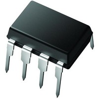
PIC12LCE673-04I/P Microchip Technology, PIC12LCE673-04I/P Datasheet - Page 41

PIC12LCE673-04I/P
Manufacturer Part Number
PIC12LCE673-04I/P
Description
IC MCU OTP 1KX14 LV A/D EE 8DIP
Manufacturer
Microchip Technology
Series
PIC® 12Cr
Specifications of PIC12LCE673-04I/P
Core Processor
PIC
Core Size
8-Bit
Speed
4MHz
Peripherals
POR, WDT
Number Of I /o
5
Program Memory Size
1.75KB (1K x 14)
Program Memory Type
OTP
Eeprom Size
16 x 8
Ram Size
128 x 8
Voltage - Supply (vcc/vdd)
2.5 V ~ 5.5 V
Data Converters
A/D 4x8b
Oscillator Type
Internal
Operating Temperature
-40°C ~ 85°C
Package / Case
8-DIP (0.300", 7.62mm)
Processor Series
PIC12LC
Core
PIC
Data Bus Width
8 bit
Data Ram Size
128 B
Maximum Clock Frequency
4 MHz
Number Of Programmable I/os
5
Number Of Timers
8
Operating Supply Voltage
2.5 V to 5.5 V
Maximum Operating Temperature
+ 85 C
Mounting Style
Through Hole
3rd Party Development Tools
52715-96, 52716-328, 52717-734
Development Tools By Supplier
ICE2000
Minimum Operating Temperature
- 40 C
On-chip Adc
8
Data Rom Size
128 B
Height
3.3 mm
Length
9.27 mm
Supply Voltage (max)
5.5 V
Supply Voltage (min)
2.5 V
Width
6.35 mm
Lead Free Status / RoHS Status
Lead free / RoHS Compliant
Connectivity
-
Lead Free Status / Rohs Status
Details
Available stocks
Company
Part Number
Manufacturer
Quantity
Price
Part Number:
PIC12LCE673-04I/P
Manufacturer:
MICROCHIP/微芯
Quantity:
20 000
7.2
When an external clock input is used for Timer0, it must
meet certain requirements. The requirements ensure
the external clock can be synchronized with the internal
phase clock (T
incrementing of Timer0 after synchronization.
7.2.1
When no prescaler is used, the external clock input is
used as the clock source. The synchronization of
T0CKI with the internal phase clocks is accomplished
by sampling the prescaler output on the Q2 and Q4
cycles of the internal phase clocks (Figure 7-5). There-
fore, it is necessary for T0CKI to be high for at least
2T
least 2T
the electrical specification of the desired device.
When a prescaler is used, the external clock input is
divided by the asynchronous ripple-counter type pres-
FIGURE 7-5:
1999 Microchip Technology Inc.
OSC
Note 1:
(and a small RC delay of 20 ns) and low for at
OSC
Using Timer0 with an External Clock
EXTERNAL CLOCK SYNCHRONIZATION
2:
3:
(and a small RC delay of 20 ns). Refer to
Delay from clock input change to Timer0 increment is 3T
in measuring the interval between two edges on Timer0 input = ±4T
External clock if no prescaler selected; prescaler output otherwise.
The arrows indicate the points in time where sampling occurs.
OSC
External Clock Input or
Prescaler output
External Clock/Prescaler
Output after sampling
Increment Timer0 (Q4)
TIMER0 TIMING WITH EXTERNAL CLOCK
). Also, there is a delay in the actual
(2)
Timer0
Q1
(3)
Q2
Q3
(1)
Q4
Q1
T0
Q2
OSC
caler, so that the prescaler output is symmetrical. For
the external clock to meet the sampling requirement,
the ripple-counter must be taken into account. There-
fore, it is necessary for T0CKI to have a period of at
least 4T
the prescaler value. The only requirement on T0CKI
high and low time is that they do not violate the mini-
mum pulse width requirement of 10 ns. Refer to param-
eters 40, 41 and 42 in the electrical specification of the
desired device.
7.2.2
Since the prescaler output is synchronized with the
internal clocks, there is a small delay from the time the
external clock edge occurs to the time the Timer0 mod-
ule is actually incremented. Figure 7-5 shows the delay
from the external clock edge to the timer incrementing.
Q3
to 7T
Q4
OSC
OSC
TMR0 INCREMENT DELAY
OSC
Q1
. (Duration of Q = T
(and a small RC delay of 40 ns) divided by
T0 + 1
max.
Q2
Q3
Q4
PIC12C67X
OSC
Q1
). Therefore, the error
Q2
T0 + 2
Small pulse
misses sampling
DS30561B-page 41
Q3
Q4


