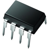
PIC12LCE673-04I/P Microchip Technology, PIC12LCE673-04I/P Datasheet - Page 14

PIC12LCE673-04I/P
Manufacturer Part Number
PIC12LCE673-04I/P
Description
IC MCU OTP 1KX14 LV A/D EE 8DIP
Manufacturer
Microchip Technology
Series
PIC® 12Cr
Specifications of PIC12LCE673-04I/P
Core Processor
PIC
Core Size
8-Bit
Speed
4MHz
Peripherals
POR, WDT
Number Of I /o
5
Program Memory Size
1.75KB (1K x 14)
Program Memory Type
OTP
Eeprom Size
16 x 8
Ram Size
128 x 8
Voltage - Supply (vcc/vdd)
2.5 V ~ 5.5 V
Data Converters
A/D 4x8b
Oscillator Type
Internal
Operating Temperature
-40°C ~ 85°C
Package / Case
8-DIP (0.300", 7.62mm)
Processor Series
PIC12LC
Core
PIC
Data Bus Width
8 bit
Data Ram Size
128 B
Maximum Clock Frequency
4 MHz
Number Of Programmable I/os
5
Number Of Timers
8
Operating Supply Voltage
2.5 V to 5.5 V
Maximum Operating Temperature
+ 85 C
Mounting Style
Through Hole
3rd Party Development Tools
52715-96, 52716-328, 52717-734
Development Tools By Supplier
ICE2000
Minimum Operating Temperature
- 40 C
On-chip Adc
8
Data Rom Size
128 B
Height
3.3 mm
Length
9.27 mm
Supply Voltage (max)
5.5 V
Supply Voltage (min)
2.5 V
Width
6.35 mm
Lead Free Status / RoHS Status
Lead free / RoHS Compliant
Connectivity
-
Lead Free Status / Rohs Status
Details
Available stocks
Company
Part Number
Manufacturer
Quantity
Price
Part Number:
PIC12LCE673-04I/P
Manufacturer:
MICROCHIP/微芯
Quantity:
20 000
PIC12C67X
TABLE 4-1:
DS30561B-page 14
80h
81h
82h
83h
84h
85h
86h
87h
88h
89h
8Ah
8Bh
8Ch
8Dh
8Eh
8Fh
90h
91h
92h
93h
94h
95h
96h
97h
98h
99h
9Ah
9Bh
9Ch
9Dh
9Eh
9Fh
Legend: x = unknown, u = unchanged, q = value depends on condition, - = unimplemented read as ’0’.
Note 1: These registers can be addressed from either bank.
Address
Bank 1
(1)
(1)
(1)
(1)
(1,2)
(1)
2: The upper byte of the program counter is not directly accessible. PCLATH is a holding register for the PC<12:8> whose con-
3: Other (non power-up) resets include external reset through MCLR and Watchdog Timer Reset.
4: The IRP and RP1 bits are reserved on the PIC12C67X; always maintain these bits clear.
5: The SCL (GP7) and SDA (GP6) bits are unimplemented on the PIC12C671/672 and read as ’0’.
INDF
OPTION
PCL
STATUS
FSR
TRIS
PCLATH
INTCON
PIE1
PCON
OSCCAL
ADCON1
Shaded locations are unimplemented, read as ‘0’.
tents are transferred to the upper byte of the program counter.
Name
—
—
—
—
—
—
—
—
—
—
—
—
—
—
—
—
—
—
—
—
PIC12C67X SPECIAL FUNCTION REGISTER SUMMARY (CONT.)
Addressing this location uses contents of FSR to address data memory (not a physical register)
Program Counter’s (PC) Least Significant Byte
Indirect data memory address pointer
Unimplemented
Unimplemented
Unimplemented
Unimplemented
Unimplemented
Unimplemented
Unimplemented
Unimplemented
Unimplemented
Unimplemented
Unimplemented
Unimplemented
Unimplemented
Unimplemented
Unimplemented
Unimplemented
Unimplemented
Unimplemented
Unimplemented
Unimplemented
GPPU
IRP
CAL3
Bit 7
GIE
—
—
—
—
—
(4)
INTEDG
RP1
CAL2
PEIE
ADIE
Bit 6
—
—
—
—
(4)
GPIO Data Direction Register
T0CS
CAL1
Bit 5
T0IE
RP0
—
—
—
—
Write Buffer for the upper 5 bits of the PC
T0SE
CAL0
INTE
Bit 4
TO
—
—
—
CALFST
GPIE
Bit 3
PSA
PD
—
—
—
CALSLW
PCFG2
Bit 2
T0IF
PS2
—
—
Z
PCFG1
Bit 1
INTF
POR
PS1
DC
—
—
1999 Microchip Technology Inc.
PCFG0
GPIF
Bit 0
PS0
—
—
—
C
1111 1111
0001 1xxx
--11 1111
---0 0000
-0-- ----
---- --0-
0111 00--
---- -000
0000 0000
0000 0000
xxxx xxxx
0000 000x
Power-on
Value on
Reset
—
—
—
—
—
—
—
—
—
—
—
—
—
—
—
—
—
—
—
—
0000 0000
1111 1111
0000 0000
000q quuu
uuuu uuuu
--11 1111
---0 0000
0000 000u
-0-- ----
---- --u-
uuuu uu--
---- -000
Resets
Value on
all other
—
—
—
—
—
—
—
—
—
—
—
—
—
—
—
—
—
—
—
—
(3)


