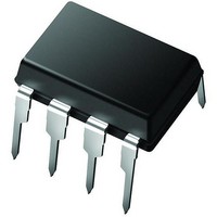
PIC12LCE673-04I/P Microchip Technology, PIC12LCE673-04I/P Datasheet - Page 33

PIC12LCE673-04I/P
Manufacturer Part Number
PIC12LCE673-04I/P
Description
IC MCU OTP 1KX14 LV A/D EE 8DIP
Manufacturer
Microchip Technology
Series
PIC® 12Cr
Specifications of PIC12LCE673-04I/P
Core Processor
PIC
Core Size
8-Bit
Speed
4MHz
Peripherals
POR, WDT
Number Of I /o
5
Program Memory Size
1.75KB (1K x 14)
Program Memory Type
OTP
Eeprom Size
16 x 8
Ram Size
128 x 8
Voltage - Supply (vcc/vdd)
2.5 V ~ 5.5 V
Data Converters
A/D 4x8b
Oscillator Type
Internal
Operating Temperature
-40°C ~ 85°C
Package / Case
8-DIP (0.300", 7.62mm)
Processor Series
PIC12LC
Core
PIC
Data Bus Width
8 bit
Data Ram Size
128 B
Maximum Clock Frequency
4 MHz
Number Of Programmable I/os
5
Number Of Timers
8
Operating Supply Voltage
2.5 V to 5.5 V
Maximum Operating Temperature
+ 85 C
Mounting Style
Through Hole
3rd Party Development Tools
52715-96, 52716-328, 52717-734
Development Tools By Supplier
ICE2000
Minimum Operating Temperature
- 40 C
On-chip Adc
8
Data Rom Size
128 B
Height
3.3 mm
Length
9.27 mm
Supply Voltage (max)
5.5 V
Supply Voltage (min)
2.5 V
Width
6.35 mm
Lead Free Status / RoHS Status
Lead free / RoHS Compliant
Connectivity
-
Lead Free Status / Rohs Status
Details
Available stocks
Company
Part Number
Manufacturer
Quantity
Price
Part Number:
PIC12LCE673-04I/P
Manufacturer:
MICROCHIP/微芯
Quantity:
20 000
6.0
The PIC12CE673 and PIC12CE674 each have 16
bytes of EEPROM data memory. The EEPROM mem-
ory has an endurance of 1,000,000 erase/write cycles
and a data retention of greater than 40 years. The
EEPROM data memory supports a bi-directional 2-wire
bus and data transmission protocol. These two-wires
are serial data (SDA) and serial clock (SCL), that are
mapped to bit6 and bit7, respectively, of the GPIO reg-
ister (SFR 06h). Unlike the GP0-GP5 that are con-
nected to the I/O pins, SDA and SCL are only
connected to the internal EEPROM peripheral. For
most applications, all that is required is calls to the
following functions:
; Byte_Write: Byte write routine
;
;
;
;
; Read_Current: Read EEPROM at address
currently held by EE device.
;
;
;
;
; Read_Random: Read EEPROM byte at supplied
address
;
;
;
The code for these functions is available on our web
site (www.microchip.com). The code will be accessed
by either including the source code FL67XINC.ASM or
by linking FLASH67X.ASM. FLASH67X.INC provides
external definition to the calling program.
6.0.1
SDA is a bi-directional pin used to transfer addresses
and data into and data out of the device.
For normal data transfer, SDA is allowed to change only
during SCL low. Changes during SCL high are
reserved for indicating the START and STOP condi-
tions.
6.0.2
This SCL signal is used to synchronize the data trans-
fer from and to the EEPROM.
1999 Microchip Technology Inc.
EEPROM PERIPHERAL
OPERATION
Inputs: EEPROM Address
Outputs:
Inputs: NONE
Outputs:
Inputs: EEPROM Address
Outputs:
SERIAL DATA
SERIAL CLOCK
EEPROM Data
Return 01 in W if OK, else
return 00 in W
EEPROM Data
Return 01 in W if OK, else
return 00 in W
EEPROM Data
Return 01 in W if OK,
else return 00 in W
EEADDR
EEDATA
EEDATA
EEADDR
EEDATA
6.1
The following bus protocol is to be used with the
EEPROM data memory. In this section, the term “proces-
sor” is used to denote the portion of the PIC12C67X that
interfaces to the EEPROM via software.
• Data transfer may be initiated only when the bus
During data transfer, the data line must remain stable
whenever the clock line is HIGH. Changes in the data
line while the clock line is HIGH will be interpreted as a
START or STOP condition.
Accordingly, the following bus conditions have been
defined (Figure 6-3).
6.1.1
Both data and clock lines remain HIGH.
6.1.2
A HIGH to LOW transition of the SDA line while the
clock (SCL) is HIGH determines a START condition. All
commands must be preceded by a START condition.
6.1.3
A LOW to HIGH transition of the SDA line while the
clock (SCL) is HIGH determines a STOP condition. All
operations must be ended with a STOP condition.
6.1.4
The state of the data line represents valid data when,
after a START condition, the data line is stable for the
duration of the HIGH period of the clock signal.
The data on the line must be changed during the LOW
period of the clock signal. There is one bit of data per
clock pulse.
Each data transfer is initiated with a START condition
and terminated with a STOP condition. The number of
the data bytes transferred between the START and
STOP conditions is determined by the available data
EEPROM space.
is not busy.
Bus Characteristics
BUS NOT BUSY (A)
START DATA TRANSFER (B)
STOP DATA TRANSFER (C)
DATA VALID (D)
PIC12C67X
DS30561B-page 33


