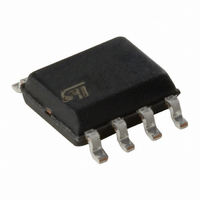
ST7FLITEU05M6 STMicroelectronics, ST7FLITEU05M6 Datasheet - Page 95

ST7FLITEU05M6
Manufacturer Part Number
ST7FLITEU05M6
Description
MCU 8BIT SGL VOLT FLASH SO-8
Manufacturer
STMicroelectronics
Series
ST7r
Datasheet
1.ST7FLITEU05M6.pdf
(139 pages)
Specifications of ST7FLITEU05M6
Core Processor
ST7
Core Size
8-Bit
Speed
8MHz
Peripherals
LVD, POR, PWM, WDT
Number Of I /o
5
Program Memory Size
2KB (2K x 8)
Program Memory Type
FLASH
Ram Size
128 x 8
Voltage - Supply (vcc/vdd)
2.4 V ~ 5.5 V
Data Converters
A/D 5x10b
Oscillator Type
Internal
Operating Temperature
-40°C ~ 85°C
Package / Case
8-SOIC (3.9mm Width)
Processor Series
ST7FLITEUx
Core
ST7
Data Bus Width
8 bit
Data Ram Size
128 B
Interface Type
ICC
Maximum Clock Frequency
4 MHz
Number Of Programmable I/os
5
Number Of Timers
2
Maximum Operating Temperature
+ 85 C
Mounting Style
SMD/SMT
Development Tools By Supplier
ST7FUS-PRIMER, ST7FLITE-SK/RAIS, ST7FLITU0-D/RAIS, STX-RLINK
Minimum Operating Temperature
- 40 C
On-chip Adc
10 bit, 5 Channel
For Use With
497-5858 - EVAL BOARD PLAYBACK ST7FLITE
Lead Free Status / RoHS Status
Lead free / RoHS Compliant
Eeprom Size
-
Connectivity
-
Lead Free Status / Rohs Status
Details
ST7LITEU05 ST7LITEU09
13
13.1
13.1.1
13.1.2
13.1.3
13.1.4
13.1.5
Electrical characteristics
Parameter conditions
Unless otherwise specified, all voltages are referred to V
Minimum and maximum values
Unless otherwise specified the minimum and maximum values are guaranteed in the worst
conditions of ambient temperature, supply voltage and frequencies by tests in production on
100 % of the devices with an ambient temperature at T
selected temperature range).
Data based on characterization results, design simulation and/or technology characteristics
are indicated in the table footnotes and are not tested in production. Based on
characterization, the minimum and maximum values refer to sample tests and represent the
mean value plus or minus three times the standard deviation (mean±3 ).
Typical values
Unless otherwise specified, typical data are based on T
4.5 V V
V
and are not tested.
Typical curves
Unless otherwise specified, all typical curves are given only as design guidelines and are
not tested.
Loading capacitor
The loading conditions used for pin parameter measurement are shown in
Figure 41. Pin loading conditions
Pin input voltage
The input voltage measurement on a pin of the device is described in
DD
=2.7 V (for the 2.4 V V
DD
5.5 V voltage range), V
DD
3 V voltage range). They are given only as design guidelines
C
L
DD
= 3.75 V (for the 3 V V
ST7 PIN
A
=25 °C and T
A
=25 °C, V
SS
.
DD
4.5 V voltage range) and
Electrical characteristics
DD
A
= 5 V (for the
=T
Figure
A
max (given by the
Figure
42.
41.
95/139


