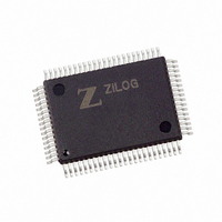
Z8F4823FT020SG Zilog, Z8F4823FT020SG Datasheet - Page 175

Z8F4823FT020SG
Manufacturer Part Number
Z8F4823FT020SG
Description
IC ENCORE MCU FLASH 48K 80QFP
Manufacturer
Zilog
Series
Encore!® XP®r
Specifications of Z8F4823FT020SG
Core Processor
Z8
Core Size
8-Bit
Speed
20MHz
Connectivity
I²C, IrDA, SPI, UART/USART
Peripherals
Brown-out Detect/Reset, DMA, POR, PWM, WDT
Number Of I /o
60
Program Memory Size
48KB (48K x 8)
Program Memory Type
FLASH
Ram Size
4K x 8
Voltage - Supply (vcc/vdd)
3 V ~ 3.6 V
Data Converters
A/D 12x10b
Oscillator Type
Internal
Operating Temperature
0°C ~ 70°C
Package / Case
80-BQFP
Processor Series
Z8F482x
Core
eZ8
Data Bus Width
8 bit
Data Ram Size
4 KB
Interface Type
I2C, SPI, UART
Maximum Clock Frequency
20 MHz
Number Of Programmable I/os
60
Number Of Timers
4
Operating Supply Voltage
3 V to 3.6 V
Maximum Operating Temperature
+ 70 C
Mounting Style
SMD/SMT
Minimum Operating Temperature
0 C
On-chip Adc
10 bit, 12 Channel
Lead Free Status / RoHS Status
Lead free / RoHS Compliant
Eeprom Size
-
Lead Free Status / Rohs Status
Details
Other names
269-4275
Z8F4823FT020SG
Z8F4823FT020SG
Available stocks
Company
Part Number
Manufacturer
Quantity
Price
- Current page: 175 of 297
- Download datasheet (9Mb)
Direct Memory Access Controller
Operation
PS019921-0308
DMA0 and DMA1 Operation
Configuring DMA0 and DMA1 for Data Transfer
The Z8 Encore! XP
three independent Direct Memory Access channels. Two of the channels (DMA0 and
DMA1) transfer data between the on-chip peripherals and the Register File. The third
channel (DMA_ADC) controls the ADC operation and transfers SINGLE-SHOT mode
ADC output data to the Register File.
DMA0 and DMA1, referred to collectively as DMAx, transfer data either from the on-chip
peripheral control registers to the Register File, or from the Register File to the on-chip
peripheral control registers. The sequence of operations in a DMAx data transfer is:
1. DMAx trigger source requests a DMA data transfer.
2. DMAx requests control of the system bus (address and data) from the eZ8 CPU.
3. After the eZ8 CPU acknowledges the bus request, DMAx transfers either a single byte
4. If Current Address equals End Address:
Follow the steps below to configure and enable DMA0 or DMA1:
1. Write to the DMAx I/O Address register to set the Register File address identifying the
2. Determine the 12-bit Start and End Register File addresses. The 12-bit Start Address
or a two-byte word (depending upon configuration) and then returns system bus
control back to the eZ8 CPU.
–
–
–
If Current Address does not equal End Address, the Current Address increments by 1
(single-byte transfer) or 2 (two-byte word transfer).
on-chip peripheral control register. The upper nibble of the 12-bit address for on-chip
peripheral control registers is always
is given by {DMAx_H[3:0], DMA_START[7:0]}. The 12-bit End Address is given by
{DMAx_H[7:4], DMA_END[7:0]}.
DMAx reloads the original Start Address
If configured to generate an interrupt, DMAx sends an interrupt request to the
Interrupt Controller
If configured for single-pass operation, DMAx resets the DEN bit in the DMAx
Control register to 0 and the DMA is disabled.
®
F64XX Series Direct Memory Access (DMA) Controller provides
FH
. The full address is {FH, DMAx_IO[7:0]}.
Z8 Encore! XP
Direct Memory Access Controller
Product Specification
®
F64XX Series
161
Related parts for Z8F4823FT020SG
Image
Part Number
Description
Manufacturer
Datasheet
Request
R

Part Number:
Description:
Communication Controllers, ZILOG INTELLIGENT PERIPHERAL CONTROLLER (ZIP)
Manufacturer:
Zilog, Inc.
Datasheet:

Part Number:
Description:
KIT DEV FOR Z8 ENCORE 16K TO 64K
Manufacturer:
Zilog
Datasheet:

Part Number:
Description:
KIT DEV Z8 ENCORE XP 28-PIN
Manufacturer:
Zilog
Datasheet:

Part Number:
Description:
DEV KIT FOR Z8 ENCORE 8K/4K
Manufacturer:
Zilog
Datasheet:

Part Number:
Description:
KIT DEV Z8 ENCORE XP 28-PIN
Manufacturer:
Zilog
Datasheet:

Part Number:
Description:
DEV KIT FOR Z8 ENCORE 4K TO 8K
Manufacturer:
Zilog
Datasheet:

Part Number:
Description:
CMOS Z8 microcontroller. ROM 16 Kbytes, RAM 256 bytes, speed 16 MHz, 32 lines I/O, 3.0V to 5.5V
Manufacturer:
Zilog, Inc.
Datasheet:

Part Number:
Description:
Low-cost microcontroller. 512 bytes ROM, 61 bytes RAM, 8 MHz
Manufacturer:
Zilog, Inc.
Datasheet:

Part Number:
Description:
Z8 4K OTP Microcontroller
Manufacturer:
Zilog, Inc.
Datasheet:

Part Number:
Description:
CMOS SUPER8 ROMLESS MCU
Manufacturer:
Zilog, Inc.
Datasheet:

Part Number:
Description:
SL1866 CMOSZ8 OTP Microcontroller
Manufacturer:
Zilog, Inc.
Datasheet:

Part Number:
Description:
SL1866 CMOSZ8 OTP Microcontroller
Manufacturer:
Zilog, Inc.
Datasheet:

Part Number:
Description:
OTP (KB) = 1, RAM = 125, Speed = 12, I/O = 14, 8-bit Timers = 2, Comm Interfaces Other Features = Por, LV Protect, Voltage = 4.5-5.5V
Manufacturer:
Zilog, Inc.
Datasheet:

Part Number:
Description:
Manufacturer:
Zilog, Inc.
Datasheet:


