Z8F4823FT020SG Zilog, Z8F4823FT020SG Datasheet - Page 219
Z8F4823FT020SG
Manufacturer Part Number
Z8F4823FT020SG
Description
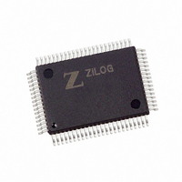
IC ENCORE MCU FLASH 48K 80QFP
Manufacturer
Zilog
Series
Encore!® XP®r
Specifications of Z8F4823FT020SG
Core Processor
Z8
Core Size
8-Bit
Speed
20MHz
Connectivity
I²C, IrDA, SPI, UART/USART
Peripherals
Brown-out Detect/Reset, DMA, POR, PWM, WDT
Number Of I /o
60
Program Memory Size
48KB (48K x 8)
Program Memory Type
FLASH
Ram Size
4K x 8
Voltage - Supply (vcc/vdd)
3 V ~ 3.6 V
Data Converters
A/D 12x10b
Oscillator Type
Internal
Operating Temperature
0°C ~ 70°C
Package / Case
80-BQFP
Processor Series
Z8F482x
Core
eZ8
Data Bus Width
8 bit
Data Ram Size
4 KB
Interface Type
I2C, SPI, UART
Maximum Clock Frequency
20 MHz
Number Of Programmable I/os
60
Number Of Timers
4
Operating Supply Voltage
3 V to 3.6 V
Maximum Operating Temperature
+ 70 C
Mounting Style
SMD/SMT
Minimum Operating Temperature
0 C
On-chip Adc
10 bit, 12 Channel
Lead Free Status / RoHS Status
Lead free / RoHS Compliant
Eeprom Size
-
Lead Free Status / Rohs Status
Details
Other names
269-4275
Z8F4823FT020SG
Z8F4823FT020SG
Available stocks
Company
Part Number
Manufacturer
Quantity
Price


On-Chip Debugger Control Register Definitions
PS019921-0308
Table 102. OCD Control Register (OCDCTL)
BITS
FIELD
RESET
R/W
OCD Control Register
DBGMODE
7
The OCD Control register
register enters or exits DEBUG mode and enables the BRK instruction.
A ‘reset and stop’ function can be achieved by writing
go’ function can be achieved by writing
mode, a ‘run’ function can be implemented by writing
DBGMODE—DEBUG Mode
Setting this bit to 1 causes the device to enter DEBUG mode. When in DEBUG mode, the
eZ8 CPU stops fetching new instructions. Clearing this bit causes the eZ8 CPU to start
running again. This bit is automatically set when a BRK instruction is decoded and Break-
points are enabled. If the Read Protect Option Bit is enabled, this bit can only be cleared
by resetting the device, it cannot be written to 0.
0 = TheZ8 Encore! XP
1 = The Z8 Encore! XP
BRKEN—Breakpoint Enable
This bit controls the behavior of the BRK instruction (opcode 00H). By default, Break-
points are disabled and the BRK instruction behaves like a NOP. If this bit is set to 1 and a
BRK instruction is decoded, the OCD takes action dependent upon the BRKLOOP bit.
0 = BRK instruction is disabled.
1 = BRK instruction is enabled.
DBGACK—Debug Acknowledge
This bit enables the debug acknowledge feature. If this bit is set to 1, then the OCD sends
an Debug Acknowledge character (
0 = Debug Acknowledge is disabled.
1 = Debug Acknowledge is enabled.
BRKLOOP—Breakpoint Loop
This bit determines what action the OCD takes when a BRK instruction is decoded if
breakpoints are enabled (BRKEN is 1). If this bit is 0, then the DBGMODE bit is automat-
ically set to 1 and the OCD entered DEBUG mode. If BRKLOOP is set to 1, then the
eZ8 CPU loops on the BRK instruction.
BRKEN
R/W
6
DBGACK BRKLOOP
®
®
5
F64XX Series device is operating in NORMAL mode.
F64XX Series device is in DEBUG mode.
(Table
102) controls the state of the On-Chip Debugger. This
FFH
4
) to the host when a Breakpoint occurs.
41H
0
to this register. If the device is in DEBUG
3
R
40H
81H
Z8 Encore! XP
to this register.
to this register. A ‘reset and
2
Product Specification
Reserved
1
®
On-Chip Debugger
F64XX Series
RST
R/W
0
205
Related parts for Z8F4823FT020SG
Image
Part Number
Description
Manufacturer
Datasheet
Request
R

Part Number:
Description:
Communication Controllers, ZILOG INTELLIGENT PERIPHERAL CONTROLLER (ZIP)
Manufacturer:
Zilog, Inc.
Datasheet:

Part Number:
Description:
KIT DEV FOR Z8 ENCORE 16K TO 64K
Manufacturer:
Zilog
Datasheet:

Part Number:
Description:
KIT DEV Z8 ENCORE XP 28-PIN
Manufacturer:
Zilog
Datasheet:

Part Number:
Description:
DEV KIT FOR Z8 ENCORE 8K/4K
Manufacturer:
Zilog
Datasheet:

Part Number:
Description:
KIT DEV Z8 ENCORE XP 28-PIN
Manufacturer:
Zilog
Datasheet:

Part Number:
Description:
DEV KIT FOR Z8 ENCORE 4K TO 8K
Manufacturer:
Zilog
Datasheet:
Part Number:
Description:
CMOS Z8 microcontroller. ROM 16 Kbytes, RAM 256 bytes, speed 16 MHz, 32 lines I/O, 3.0V to 5.5V
Manufacturer:
Zilog, Inc.
Datasheet:
Part Number:
Description:
Low-cost microcontroller. 512 bytes ROM, 61 bytes RAM, 8 MHz
Manufacturer:
Zilog, Inc.
Datasheet:
Part Number:
Description:
Z8 4K OTP Microcontroller
Manufacturer:
Zilog, Inc.
Datasheet:
Part Number:
Description:
CMOS SUPER8 ROMLESS MCU
Manufacturer:
Zilog, Inc.
Datasheet:
Part Number:
Description:
SL1866 CMOSZ8 OTP Microcontroller
Manufacturer:
Zilog, Inc.
Datasheet:
Part Number:
Description:
SL1866 CMOSZ8 OTP Microcontroller
Manufacturer:
Zilog, Inc.
Datasheet:
Part Number:
Description:
OTP (KB) = 1, RAM = 125, Speed = 12, I/O = 14, 8-bit Timers = 2, Comm Interfaces Other Features = Por, LV Protect, Voltage = 4.5-5.5V
Manufacturer:
Zilog, Inc.
Datasheet:
Part Number:
Description:
Manufacturer:
Zilog, Inc.
Datasheet: