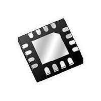
MC9S08QG84CFFER Freescale Semiconductor, MC9S08QG84CFFER Datasheet - Page 166

MC9S08QG84CFFER
Manufacturer Part Number
MC9S08QG84CFFER
Description
IC MCU 8BIT 8K FLASH 16-QFN
Manufacturer
Freescale Semiconductor
Series
HCS08r
Datasheet
1.MC9S08QG8CDTER.pdf
(314 pages)
Specifications of MC9S08QG84CFFER
Core Processor
HCS08
Core Size
8-Bit
Speed
20MHz
Connectivity
I²C, SCI, SPI
Peripherals
LVD, POR, PWM, WDT
Number Of I /o
12
Program Memory Size
8KB (8K x 8)
Program Memory Type
FLASH
Ram Size
512 x 8
Voltage - Supply (vcc/vdd)
1.8 V ~ 3.6 V
Data Converters
A/D 8x10b
Oscillator Type
Internal
Operating Temperature
-40°C ~ 85°C
Package / Case
16-QFN
Data Bus Width
8 bit
Maximum Clock Frequency
20 MHz
Data Ram Size
512 B
On-chip Adc
Yes
Number Of Programmable I/os
12
Number Of Timers
1
Mounting Style
SMD/SMT
Height
1 mm
Interface Type
I2C, SCI, SPI
Length
5 mm
Maximum Operating Temperature
+ 85 C
Minimum Operating Temperature
- 40 C
Supply Voltage (max)
3.6 V
Supply Voltage (min)
1.8 V
Width
5 mm
For Use With
DEMO9S08QG8E - BOARD DEMO FOR MC9S08QG8
Lead Free Status / RoHS Status
Lead free / RoHS Compliant
Eeprom Size
-
Lead Free Status / Rohs Status
Details
- Current page: 166 of 314
- Download datasheet (6Mb)
Inter-Integrated Circuit (S08IICV1)
11.3.5
In slave mode, the same functions are available after an address match has occurred.
Note that the TX bit in IICC must correctly reflect the desired direction of transfer in master and slave
modes for the transmission to begin. For instance, if the IIC is configured for master transmit but a master
receive is desired, then reading the IICD will not initiate the receive.
Reading the IICD will return the last byte received while the IIC is configured in either master receive or
slave receive modes. The IICD does not reflect every byte that is transmitted on the IIC bus, nor can
software verify that a byte has been written to the IICD correctly by reading it back.
In master transmit mode, the first byte of data written to IICD following assertion of MST is used for the
address transfer and should comprise of the calling address (in bit 7–bit 1) concatenated with the required
R/W bit (in position bit 0).
164
Reset
Field
DATA
7:0
W
R
IIC Data I/O Register (IICD)
Data — In master transmit mode, when data is written to the IICD, a data transfer is initiated. The most significant
bit is sent first. In master receive mode, reading this register initiates receiving of the next byte of data.
0
7
When transmitting out of master receive mode, the IIC mode should be
switched before reading the IICD register to prevent an inadvertent
initiation of a master receive data transfer.
0
6
MC9S08QG8 and MC9S08QG4 Data Sheet, Rev. 5
Table 11-7. IICD Register Field Descriptions
Figure 11-7. IIC Data I/O Register (IICD)
0
5
NOTE
0
4
Description
DATA
3
0
0
2
Freescale Semiconductor
0
1
0
0
Related parts for MC9S08QG84CFFER
Image
Part Number
Description
Manufacturer
Datasheet
Request
R
Part Number:
Description:
Hcs08 Microcontrollers
Manufacturer:
Freescale Semiconductor, Inc
Datasheet:
Part Number:
Description:
Manufacturer:
Freescale Semiconductor, Inc
Datasheet:
Part Number:
Description:
Manufacturer:
Freescale Semiconductor, Inc
Datasheet:
Part Number:
Description:
Manufacturer:
Freescale Semiconductor, Inc
Datasheet:
Part Number:
Description:
Manufacturer:
Freescale Semiconductor, Inc
Datasheet:
Part Number:
Description:
Manufacturer:
Freescale Semiconductor, Inc
Datasheet:
Part Number:
Description:
Manufacturer:
Freescale Semiconductor, Inc
Datasheet:
Part Number:
Description:
Manufacturer:
Freescale Semiconductor, Inc
Datasheet:
Part Number:
Description:
Manufacturer:
Freescale Semiconductor, Inc
Datasheet:
Part Number:
Description:
Manufacturer:
Freescale Semiconductor, Inc
Datasheet:
Part Number:
Description:
Manufacturer:
Freescale Semiconductor, Inc
Datasheet:
Part Number:
Description:
Manufacturer:
Freescale Semiconductor, Inc
Datasheet:
Part Number:
Description:
Manufacturer:
Freescale Semiconductor, Inc
Datasheet:
Part Number:
Description:
Manufacturer:
Freescale Semiconductor, Inc
Datasheet:
Part Number:
Description:
Manufacturer:
Freescale Semiconductor, Inc
Datasheet:


