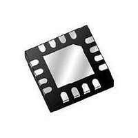
MC9S08QG84CFFER Freescale Semiconductor, MC9S08QG84CFFER Datasheet - Page 80

MC9S08QG84CFFER
Manufacturer Part Number
MC9S08QG84CFFER
Description
IC MCU 8BIT 8K FLASH 16-QFN
Manufacturer
Freescale Semiconductor
Series
HCS08r
Datasheet
1.MC9S08QG8CDTER.pdf
(314 pages)
Specifications of MC9S08QG84CFFER
Core Processor
HCS08
Core Size
8-Bit
Speed
20MHz
Connectivity
I²C, SCI, SPI
Peripherals
LVD, POR, PWM, WDT
Number Of I /o
12
Program Memory Size
8KB (8K x 8)
Program Memory Type
FLASH
Ram Size
512 x 8
Voltage - Supply (vcc/vdd)
1.8 V ~ 3.6 V
Data Converters
A/D 8x10b
Oscillator Type
Internal
Operating Temperature
-40°C ~ 85°C
Package / Case
16-QFN
Data Bus Width
8 bit
Maximum Clock Frequency
20 MHz
Data Ram Size
512 B
On-chip Adc
Yes
Number Of Programmable I/os
12
Number Of Timers
1
Mounting Style
SMD/SMT
Height
1 mm
Interface Type
I2C, SCI, SPI
Length
5 mm
Maximum Operating Temperature
+ 85 C
Minimum Operating Temperature
- 40 C
Supply Voltage (max)
3.6 V
Supply Voltage (min)
1.8 V
Width
5 mm
For Use With
DEMO9S08QG8E - BOARD DEMO FOR MC9S08QG8
Lead Free Status / RoHS Status
Lead free / RoHS Compliant
Eeprom Size
-
Lead Free Status / Rohs Status
Details
- Current page: 80 of 314
- Download datasheet (6Mb)
Chapter 6 Parallel Input/Output Control
The data direction control bit (PTxDDn) determines whether the output buffer for the associated pin is
enabled, and also controls the source for port data register reads. The input buffer for the associated pin is
always enabled unless the pin is enabled as an analog function or is an output-only pin.
When a shared digital function is enabled for a pin, the output buffer is controlled by the shared function.
However, the data direction register bit will continue to control the source for reads of the port data register.
When a shared analog function is enabled for a pin, both the input and output buffers are disabled. A value
of 0 is read for any port data bit where the bit is an input (PTxDDn = 0) and the input buffer is disabled. In
general, whenever a pin is shared with both an alternate digital function and an analog function, the analog
function has priority such that if both the digital and analog functions are enabled, the analog function
controls the pin.
It is a good programming practice to write to the port data register before changing the direction of a port
pin to become an output. This ensures that the pin will not be driven momentarily with an old data value
that happened to be in the port data register.
6.2
Associated with the parallel I/O ports is a set of registers located in the high page register space that operate
independently of the parallel I/O registers. These registers are used to control pullups, slew rate, and drive
strength for the pins.
78
Pin Control — Pullup, Slew Rate, and Drive Strength
Port Read
BUSCLK
Data
MC9S08QG8 and MC9S08QG4 Data Sheet, Rev. 5
Figure 6-1. Parallel I/O Block Diagram
PTxDDn
D
D
PTxDn
Q
Q
1
0
Synchronizer
Output Enable
Output Data
Freescale Semiconductor
Input Data
Related parts for MC9S08QG84CFFER
Image
Part Number
Description
Manufacturer
Datasheet
Request
R
Part Number:
Description:
Hcs08 Microcontrollers
Manufacturer:
Freescale Semiconductor, Inc
Datasheet:
Part Number:
Description:
Manufacturer:
Freescale Semiconductor, Inc
Datasheet:
Part Number:
Description:
Manufacturer:
Freescale Semiconductor, Inc
Datasheet:
Part Number:
Description:
Manufacturer:
Freescale Semiconductor, Inc
Datasheet:
Part Number:
Description:
Manufacturer:
Freescale Semiconductor, Inc
Datasheet:
Part Number:
Description:
Manufacturer:
Freescale Semiconductor, Inc
Datasheet:
Part Number:
Description:
Manufacturer:
Freescale Semiconductor, Inc
Datasheet:
Part Number:
Description:
Manufacturer:
Freescale Semiconductor, Inc
Datasheet:
Part Number:
Description:
Manufacturer:
Freescale Semiconductor, Inc
Datasheet:
Part Number:
Description:
Manufacturer:
Freescale Semiconductor, Inc
Datasheet:
Part Number:
Description:
Manufacturer:
Freescale Semiconductor, Inc
Datasheet:
Part Number:
Description:
Manufacturer:
Freescale Semiconductor, Inc
Datasheet:
Part Number:
Description:
Manufacturer:
Freescale Semiconductor, Inc
Datasheet:
Part Number:
Description:
Manufacturer:
Freescale Semiconductor, Inc
Datasheet:
Part Number:
Description:
Manufacturer:
Freescale Semiconductor, Inc
Datasheet:


