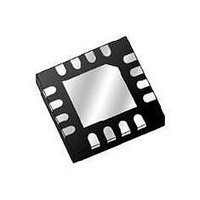
MC9S08QG84CFFER Freescale Semiconductor, MC9S08QG84CFFER Datasheet - Page 79

MC9S08QG84CFFER
Manufacturer Part Number
MC9S08QG84CFFER
Description
IC MCU 8BIT 8K FLASH 16-QFN
Manufacturer
Freescale Semiconductor
Series
HCS08r
Datasheet
1.MC9S08QG8CDTER.pdf
(314 pages)
Specifications of MC9S08QG84CFFER
Core Processor
HCS08
Core Size
8-Bit
Speed
20MHz
Connectivity
I²C, SCI, SPI
Peripherals
LVD, POR, PWM, WDT
Number Of I /o
12
Program Memory Size
8KB (8K x 8)
Program Memory Type
FLASH
Ram Size
512 x 8
Voltage - Supply (vcc/vdd)
1.8 V ~ 3.6 V
Data Converters
A/D 8x10b
Oscillator Type
Internal
Operating Temperature
-40°C ~ 85°C
Package / Case
16-QFN
Data Bus Width
8 bit
Maximum Clock Frequency
20 MHz
Data Ram Size
512 B
On-chip Adc
Yes
Number Of Programmable I/os
12
Number Of Timers
1
Mounting Style
SMD/SMT
Height
1 mm
Interface Type
I2C, SCI, SPI
Length
5 mm
Maximum Operating Temperature
+ 85 C
Minimum Operating Temperature
- 40 C
Supply Voltage (max)
3.6 V
Supply Voltage (min)
1.8 V
Width
5 mm
For Use With
DEMO9S08QG8E - BOARD DEMO FOR MC9S08QG8
Lead Free Status / RoHS Status
Lead free / RoHS Compliant
Eeprom Size
-
Lead Free Status / Rohs Status
Details
- Current page: 79 of 314
- Download datasheet (6Mb)
Chapter 6
Parallel Input/Output Control
This section explains software controls related to parallel input/output (I/O) and pin control. The
MC9S08QG8 has two parallel I/O ports which include a total of 12 I/O pins, one output-only pin and one
input-only pin. See
assignments and external hardware considerations of these pins. Not all pins are available on all devices
of the MC9S08QG8/4 Family; see
device.
All of these I/O pins are shared with on-chip peripheral functions as shown in
modules have priority over the I/Os so that when a peripheral is enabled, the I/O functions associated with
the shared pins are disabled. After reset, the shared peripheral functions are disabled so that the pins are
controlled by the I/O. All of the I/Os are configured as inputs (PTxDDn = 0) with pullup devices disabled
(PTxPEn = 0), except for output-only pin PTA4 which defaults to the BKGD/MS pin.
6.1
Reading and writing of parallel I/Os is performed through the port data registers. The direction, either input
or output, is controlled through the port data direction registers. The parallel I/O port function for an
individual pin is illustrated in the block diagram shown in
Freescale Semiconductor
Port Data and Data Direction
Not all general-purpose I/O pins are available on all packages. To avoid
extra current drain from floating input pins, the user reset initialization
routine in the application program must either enable on-chip pullup devices
or change the direction of unconnected pins to outputs so the pins do not
float.
Section Chapter 2, “External Signal
MC9S08QG8 and MC9S08QG4 Data Sheet, Rev. 5
Table 1-1
for the number of general-purpose pins available on your
NOTE
Description,” for more information about pin
Figure
6-1.
Table
2-2. The peripheral
77
Related parts for MC9S08QG84CFFER
Image
Part Number
Description
Manufacturer
Datasheet
Request
R
Part Number:
Description:
Hcs08 Microcontrollers
Manufacturer:
Freescale Semiconductor, Inc
Datasheet:
Part Number:
Description:
Manufacturer:
Freescale Semiconductor, Inc
Datasheet:
Part Number:
Description:
Manufacturer:
Freescale Semiconductor, Inc
Datasheet:
Part Number:
Description:
Manufacturer:
Freescale Semiconductor, Inc
Datasheet:
Part Number:
Description:
Manufacturer:
Freescale Semiconductor, Inc
Datasheet:
Part Number:
Description:
Manufacturer:
Freescale Semiconductor, Inc
Datasheet:
Part Number:
Description:
Manufacturer:
Freescale Semiconductor, Inc
Datasheet:
Part Number:
Description:
Manufacturer:
Freescale Semiconductor, Inc
Datasheet:
Part Number:
Description:
Manufacturer:
Freescale Semiconductor, Inc
Datasheet:
Part Number:
Description:
Manufacturer:
Freescale Semiconductor, Inc
Datasheet:
Part Number:
Description:
Manufacturer:
Freescale Semiconductor, Inc
Datasheet:
Part Number:
Description:
Manufacturer:
Freescale Semiconductor, Inc
Datasheet:
Part Number:
Description:
Manufacturer:
Freescale Semiconductor, Inc
Datasheet:
Part Number:
Description:
Manufacturer:
Freescale Semiconductor, Inc
Datasheet:
Part Number:
Description:
Manufacturer:
Freescale Semiconductor, Inc
Datasheet:


