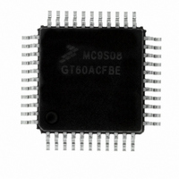
MC9S08GT60ACFBE Freescale Semiconductor, MC9S08GT60ACFBE Datasheet - Page 55

MC9S08GT60ACFBE
Manufacturer Part Number
MC9S08GT60ACFBE
Description
IC MCU 60K FLASH 4K RAM 44-QFP
Manufacturer
Freescale Semiconductor
Series
HCS08r
Datasheet
1.MC9S08GT60ACFDER.pdf
(302 pages)
Specifications of MC9S08GT60ACFBE
Core Processor
HCS08
Core Size
8-Bit
Speed
40MHz
Connectivity
I²C, SCI, SPI
Peripherals
LVD, POR, PWM, WDT
Number Of I /o
36
Program Memory Size
60KB (60K x 8)
Program Memory Type
FLASH
Ram Size
4K x 8
Voltage - Supply (vcc/vdd)
1.8 V ~ 3.6 V
Data Converters
A/D 8x10b
Oscillator Type
Internal
Operating Temperature
-40°C ~ 85°C
Package / Case
44-QFP
Cpu Family
HCS08
Device Core Size
8b
Frequency (max)
40MHz
Interface Type
I2C/SCI/SPI
Total Internal Ram Size
4KB
# I/os (max)
36
Number Of Timers - General Purpose
4
Operating Supply Voltage (typ)
2.5/3.3V
Operating Supply Voltage (max)
3.6V
Operating Supply Voltage (min)
1.8/2.08V
On-chip Adc
8-chx10-bit
Instruction Set Architecture
CISC
Operating Temp Range
-40C to 85C
Operating Temperature Classification
Industrial
Mounting
Surface Mount
Pin Count
44
Package Type
PQFP
Processor Series
S08GT
Core
HCS08
Data Bus Width
8 bit
Data Ram Size
4 KB
Maximum Clock Frequency
20 MHz
Number Of Programmable I/os
39
Number Of Timers
2
Operating Supply Voltage
0 V to 1.8 V
Maximum Operating Temperature
+ 85 C
Mounting Style
SMD/SMT
3rd Party Development Tools
EWS08
Development Tools By Supplier
M68EVB908GB60E, M68DEMO908GB60E
Minimum Operating Temperature
- 40 C
For Use With
M68DEMO908GB60E - BOARD DEMO MC9S08GB60M68EVB908GB60E - BOARD EVAL FOR MC9S08GB60
Lead Free Status / RoHS Status
Lead free / RoHS Compliant
Eeprom Size
-
Lead Free Status / Rohs Status
Compliant
Available stocks
Company
Part Number
Manufacturer
Quantity
Price
Company:
Part Number:
MC9S08GT60ACFBE
Manufacturer:
Freescale Semiconductor
Quantity:
10 000
Part Number:
MC9S08GT60ACFBE
Manufacturer:
FREESCALE深圳进口
Quantity:
20 000
Company:
Part Number:
MC9S08GT60ACFBER
Manufacturer:
Freescale Semiconductor
Quantity:
10 000
4.4.5
An access error occurs whenever the command execution protocol is violated.
Any of the following specific actions will cause the access error flag (FACCERR) in FSTAT to be set.
FACCERR must be cleared by writing a 1 to FACCERR in FSTAT before any command can be processed.
4.4.6
Block protection prevents program or erase changes for flash memory locations in a designated address
range. Mass erase is disabled when any block of flash is protected. The MC9S08GBxxA/GTxxA allows a
block of memory at the end of flash, and/or the entire flash memory to be block protected. A disable control
bit and a 3-bit control field, allows the user to set the size of this block. A separate control bit allows block
protection of the entire flash memory array. All seven of these control bits are located in the FPROT
register (see
At reset, the high-page register (FPROT) is loaded with the contents of the NVPROT location which is in
the nonvolatile register block of the flash memory. The value in FPROT cannot be changed directly from
application software so a runaway program cannot alter the block protection settings. If the last 512 bytes
of flash which includes the NVPROT register is protected, the application program cannot alter the block
protection settings (intentionally or unintentionally). The FPROT control bits can be written by
background debug commands to allow a way to erase a protected flash memory.
One use for block protection is to block protect an area of flash memory for a bootloader program. This
bootloader program then can be used to erase the rest of the flash memory and reprogram it. Because the
bootloader is protected, it remains intact even if MCU power is lost in the middle of an erase and
reprogram operation.
Freescale Semiconductor
•
•
•
•
•
•
•
•
•
•
Writing to a flash address before the internal flash clock frequency has been set by writing to the
FCDIV register
command buffer is empty.)
Writing a second time to a flash address before launching the previous command (There is only
one write to flash for every command.)
Writing a second time to FCMD before launching the previous command (There is only one write
to FCMD for every command.)
Writing to any flash control register other than FCMD after writing to a flash address
Writing any command code other than the five allowed codes (0x05, 0x20, 0x25, 0x40, or 0x41)
to FCMD
Accessing (read or write) any flash control register other than the write to FSTAT (to clear FCBEF
and launch the command) after writing the command to FCMD
The MCU enters stop mode while a program or erase command is in progress (The command is
aborted.)
Writing the byte program, burst program, or page erase command code (0x20, 0x25, or 0x40) with
a background debug command while the MCU is secured (The background debug controller can
only do blank check and mass erase commands when the MCU is secure.)
Writing 0 to FCBEF to cancel a partial command
Writing to a flash address while FCBEF is not set (A new command cannot be started until the
Access Errors
Flash Block Protection
Section 4.6.4, “Flash Protection Register (FPROT and
MC9S08GB60A Data Sheet, Rev. 2
NVPROT)”).
Chapter 4 Memory
55


