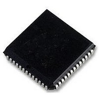
MC68HC11E1CFNE3 Freescale Semiconductor, MC68HC11E1CFNE3 Datasheet - Page 28

MC68HC11E1CFNE3
Manufacturer Part Number
MC68HC11E1CFNE3
Description
IC MCU 8BIT 3MHZ 52-PLCC
Manufacturer
Freescale Semiconductor
Series
HC11r
Specifications of MC68HC11E1CFNE3
Core Processor
HC11
Core Size
8-Bit
Speed
3MHz
Connectivity
SCI, SPI
Peripherals
POR, WDT
Number Of I /o
38
Program Memory Type
ROMless
Eeprom Size
512 x 8
Ram Size
512 x 8
Voltage - Supply (vcc/vdd)
4.5 V ~ 5.5 V
Data Converters
A/D 8x8b
Oscillator Type
Internal
Operating Temperature
-40°C ~ 85°C
Package / Case
52-PLCC
Controller Family/series
68HC11
No. Of I/o's
38
Eeprom Memory Size
512Byte
Ram Memory Size
512Byte
Cpu Speed
3MHz
No. Of Timers
1
Embedded Interface Type
SCI, SPI
Rohs Compliant
Yes
Processor Series
HC11E
Core
HC11
Data Bus Width
8 bit
Program Memory Size
512 B
Data Ram Size
512 B
Interface Type
SCI, SPI
Maximum Clock Frequency
3 MHz
Number Of Programmable I/os
22
Number Of Timers
8
Operating Supply Voltage
3 V to 5 V
Maximum Operating Temperature
+ 70 C
Mounting Style
SMD/SMT
Minimum Operating Temperature
0 C
On-chip Adc
8 bit, 8 Channel
Lead Free Status / RoHS Status
Lead free / RoHS Compliant
Program Memory Size
-
Lead Free Status / Rohs Status
Details
Available stocks
Company
Part Number
Manufacturer
Quantity
Price
Company:
Part Number:
MC68HC11E1CFNE3
Manufacturer:
NXP
Quantity:
447
Company:
Part Number:
MC68HC11E1CFNE3
Manufacturer:
Freescale Semiconductor
Quantity:
10 000
Part Number:
MC68HC11E1CFNE3
Manufacturer:
FREESCALE
Quantity:
20 000
Company:
Part Number:
MC68HC11E1CFNE3R
Manufacturer:
ON
Quantity:
5 510
Company:
Part Number:
MC68HC11E1CFNE3R
Manufacturer:
PERICOM
Quantity:
5 510
Company:
Part Number:
MC68HC11E1CFNE3R
Manufacturer:
Freescale Semiconductor
Quantity:
10 000
General Description
1.4.15 Port D
Pins PD5–PD0 can be used for general-purpose I/O signals. These pins alternately serve as the serial
communication interface (SCI) and serial peripheral interface (SPI) signals when those subsystems are
enabled.
1.4.16 Port E
Use port E for general-purpose or analog-to-digital (A/D) inputs.
28
•
•
•
PD0 is the receive data input (RxD) signal for the SCI.
PD1 is the transmit data output (TxD) signal for the SCI.
PD5–PD2 are dedicated to the SPI:
–
–
–
–
PD2 is the master in/slave out (MISO) signal.
PD3 is the master out/slave in (MOSI) signal.
PD4 is the serial clock (SCK) signal.
PD5 is the slave select (SS) input.
If high accuracy is required for A/D conversions, avoid reading port E during
sampling, as small disturbances can reduce the accuracy of that result.
M68HC11E Family Data Sheet, Rev. 5.1
CAUTION
Freescale Semiconductor


