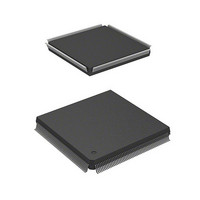
HD6417750SF167V Renesas Electronics America, HD6417750SF167V Datasheet - Page 21

HD6417750SF167V
Manufacturer Part Number
HD6417750SF167V
Description
MPU 3V 16K PB-FREE 208-QFP
Manufacturer
Renesas Electronics America
Series
SuperH® SH7750r
Datasheet
1.D6417750RBP240DV.pdf
(1164 pages)
Specifications of HD6417750SF167V
Core Processor
SH-4
Core Size
32-Bit
Speed
167MHz
Connectivity
EBI/EMI, FIFO, SCI, SmartCard
Peripherals
DMA, POR, WDT
Number Of I /o
28
Program Memory Type
ROMless
Ram Size
24K x 8
Voltage - Supply (vcc/vdd)
1.6 V ~ 2 V
Oscillator Type
External
Operating Temperature
-20°C ~ 75°C
Package / Case
208-QFP
Lead Free Status / RoHS Status
Lead free / RoHS Compliant
Eeprom Size
-
Program Memory Size
-
Data Converters
-
Available stocks
Company
Part Number
Manufacturer
Quantity
Price
Company:
Part Number:
HD6417750SF167V
Manufacturer:
INTERSIL
Quantity:
18 720
Company:
Part Number:
HD6417750SF167V
Manufacturer:
Renesas Electronics America
Quantity:
10 000
- Current page: 21 of 1164
- Download datasheet (7Mb)
Item
13.3.4 DRAM Interface
Refresh Timing:
• Self-Refresh
13.3.5 Synchronous
DRAM Interface
Page
463
465
Revision (See Manual for Details)
Description deleted
After the self-refresh is cleared, the refresh controller
immediately generates a refresh request. The RAS precharge
time immediately after the end of the self-refreshing can be set
by bits TRC2–TRC0 in MCR.
CAS-before-RAS refreshing is performed in normal operation,
in sleep mode, and in the case of a manual reset.
Description amended
With this LSI, burst read/burst write mode is supported as the
synchronous DRAM operating mode. The data bus width is 32
or 64 bits, and the SZ size bits in MCR must be set to 00 or 11.
The burst enable bit (BE) in MCR is ignored, a 32-byte burst
transfer is performed in a cache fill/copy-back cycle, and in a
write-through area write or a non-cacheable area read/write,
32-byte data is read even in a single read in order to access
synchronous DRAM with a burst read/write access. 32-byte
data transfer is also performed in a single write, but DQMn is
not asserted when unnecessary data is transferred. For details
on the burst length, see section 13.2.10, Synchronous DRAM
Mode Register (SDMR), and Power-On Sequence in section
13.3.5, Synchronous DRAM Interface. The SH7750R Group
supports burst read and burst write operations with a burst
length of 4 as a synchronous DRAM operating mode when
using a 32-bit data bus. The burst enable (BE) bit in MCR is
ignored, and a 32-byte burst transfer is performed in a cache fill
or copy-back cycle. In write-through area write operations and
non-cacheable area read or write operations, 16 bytes of data
is read even in a single read because burst read or write
accesses to synchronous DRAM use a burst length of 4.
Sixteen bytes of data is transferred in the case of a single write
also, but DQMn is not asserted when unnecessary data is
transferred.
For changing the burst length (a function only available in the
SH7750R) for a 32-bit bus, see Notes on Changing the Burst
Length (SH7750R Only) in section 13.3.5, Synchronous DRAM
Interface.
Rev.7.00 Oct. 10, 2008 Page xix of lxxxiv
REJ09B0366-0700
Related parts for HD6417750SF167V
Image
Part Number
Description
Manufacturer
Datasheet
Request
R

Part Number:
Description:
KIT STARTER FOR M16C/29
Manufacturer:
Renesas Electronics America
Datasheet:

Part Number:
Description:
KIT STARTER FOR R8C/2D
Manufacturer:
Renesas Electronics America
Datasheet:

Part Number:
Description:
R0K33062P STARTER KIT
Manufacturer:
Renesas Electronics America
Datasheet:

Part Number:
Description:
KIT STARTER FOR R8C/23 E8A
Manufacturer:
Renesas Electronics America
Datasheet:

Part Number:
Description:
KIT STARTER FOR R8C/25
Manufacturer:
Renesas Electronics America
Datasheet:

Part Number:
Description:
KIT STARTER H8S2456 SHARPE DSPLY
Manufacturer:
Renesas Electronics America
Datasheet:

Part Number:
Description:
KIT STARTER FOR R8C38C
Manufacturer:
Renesas Electronics America
Datasheet:

Part Number:
Description:
KIT STARTER FOR R8C35C
Manufacturer:
Renesas Electronics America
Datasheet:

Part Number:
Description:
KIT STARTER FOR R8CL3AC+LCD APPS
Manufacturer:
Renesas Electronics America
Datasheet:

Part Number:
Description:
KIT STARTER FOR RX610
Manufacturer:
Renesas Electronics America
Datasheet:

Part Number:
Description:
KIT STARTER FOR R32C/118
Manufacturer:
Renesas Electronics America
Datasheet:

Part Number:
Description:
KIT DEV RSK-R8C/26-29
Manufacturer:
Renesas Electronics America
Datasheet:

Part Number:
Description:
KIT STARTER FOR SH7124
Manufacturer:
Renesas Electronics America
Datasheet:

Part Number:
Description:
KIT STARTER FOR H8SX/1622
Manufacturer:
Renesas Electronics America
Datasheet:

Part Number:
Description:
KIT DEV FOR SH7203
Manufacturer:
Renesas Electronics America
Datasheet:


