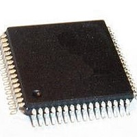
SAK-XC888CLM-8FFA 5V AC Infineon Technologies, SAK-XC888CLM-8FFA 5V AC Datasheet - Page 62

SAK-XC888CLM-8FFA 5V AC
Manufacturer Part Number
SAK-XC888CLM-8FFA 5V AC
Description
IC MCU 8BIT FLASH 64-LQFP
Manufacturer
Infineon Technologies
Series
XC8xxr
Datasheet
1.SAF-XC888CLM-6FFA_5V_AC.pdf
(144 pages)
Specifications of SAK-XC888CLM-8FFA 5V AC
Core Processor
XC800
Core Size
8-Bit
Speed
103.2MHz
Connectivity
CAN, LIN, SSI, UART/USART
Peripherals
Brown-out Detect/Reset, POR, PWM, WDT
Number Of I /o
48
Program Memory Size
32KB (32K x 8)
Program Memory Type
FLASH
Ram Size
1.75K x 8
Voltage - Supply (vcc/vdd)
4.5 V ~ 5.5 V
Data Converters
A/D 8x10b
Oscillator Type
Internal
Operating Temperature
-40°C ~ 125°C
Package / Case
64-LFQFP
Data Bus Width
8 bit
Data Ram Size
1.75 KB
Interface Type
UART, SSC
Maximum Clock Frequency
24 MHz
Number Of Programmable I/os
48
Number Of Timers
4
Operating Supply Voltage
5 V
Maximum Operating Temperature
+ 125 C
Mounting Style
SMD/SMT
Minimum Operating Temperature
- 40 C
On-chip Adc
10 bit, 8 Channel
For Use With
B158-H8743-X-X-7600IN - KIT STARTER XC886/888
Lead Free Status / RoHS Status
Lead free / RoHS Compliant
Eeprom Size
-
Lead Free Status / Rohs Status
Details
Other names
SP000210982
- Current page: 62 of 144
- Download datasheet (2Mb)
3.3.3
For the P-Flash banks, a programmed wordline (WL) must be erased before it can be
reprogrammed as the Flash cells can only withstand one gate disturb. This means that
the entire sector containing the WL must be erased since it is impossible to erase a
single WL.
For the D-Flash bank, the same WL can be programmed twice before erasing is required
as the Flash cells are able to withstand two gate disturbs. This means if the number of
data bytes that needs to be written is smaller than the 32-byte minimum programming
width, the user can opt to program this number of data bytes (x; where x can be any
integer from 1 to 31) first and program the remaining bytes (32 - x) later. Hence, it is
possible to program the same WL, for example, with 16 bytes of data two times (see
Figure
Figure 12
Note: When programming a D-Flash WL the second time, the previously programmed
Data Sheet
Flash memory cells (whether 0s or 1s) should be reprogrammed with 0s to retain
its original contents and to prevent “over-programming”.
0000 ….. 0000
0000 ….. 0000
1111 ….. 0000
12)
Flash Programming Width
Flash memory cells
D-Flash Programming
32 bytes (1 WL)
H
H
H
0000 ….. 0000
1111 ….. 1111
1111 ….. 1111
H
H
H
Program 1
Program 2
55
0000 ….. 0000
1111 ….. 0000
Note: A Flash memory cell can be programmed
16 bytes
32-byte write buffers
from 0 to 1, but not from 1 to 0.
Functional Description
H
H
XC886/888CLM
1111 ….. 1111
0000 ….. 0000
16 bytes
V1.2, 2009-07
H
H
Related parts for SAK-XC888CLM-8FFA 5V AC
Image
Part Number
Description
Manufacturer
Datasheet
Request
R

Part Number:
Description:
IC MCU 8BIT FLASH 64-LQFP
Manufacturer:
Infineon Technologies
Datasheet:

Part Number:
Description:
IC MCU 8BIT FLASH 64-TQFP
Manufacturer:
Infineon Technologies
Datasheet:

Part Number:
Description:
High Performance 8-bit Microcontroller With On-chip Flash Memory And Can
Manufacturer:
Infineon Technologies Corporation
Datasheet:

Part Number:
Description:
IC MCU 8BIT FLASH TQFP-64
Manufacturer:
Infineon Technologies
Datasheet:

Part Number:
Description:
IC MCU 8BIT FLASH 64-LQFP
Manufacturer:
Infineon Technologies
Datasheet:

Part Number:
Description:
IC MCU 8BIT FLASH 64-LQFP
Manufacturer:
Infineon Technologies
Datasheet:

Part Number:
Description:
IC MCU 8BIT FLASH 64-LQFP
Manufacturer:
Infineon Technologies
Datasheet:

Part Number:
Description:
Manufacturer:
Infineon Technologies AG
Datasheet:

Part Number:
Description:
Manufacturer:
Infineon Technologies AG
Datasheet:

Part Number:
Description:
Manufacturer:
Infineon Technologies AG
Datasheet:

Part Number:
Description:
Manufacturer:
Infineon Technologies AG
Datasheet:

Part Number:
Description:
Manufacturer:
Infineon Technologies AG
Datasheet:

Part Number:
Description:
Manufacturer:
Infineon Technologies AG
Datasheet:

Part Number:
Description:
Manufacturer:
Infineon Technologies AG
Datasheet:

Part Number:
Description:
16-bit microcontroller with 2x2 KByte RAM
Manufacturer:
Infineon Technologies AG
Datasheet:


