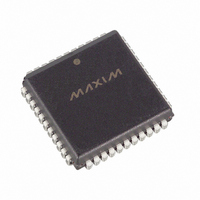
DS87C520-QNL+T&R Maxim Integrated Products, DS87C520-QNL+T&R Datasheet - Page 11

DS87C520-QNL+T&R
Manufacturer Part Number
DS87C520-QNL+T&R
Description
IC MCU EPROM/ROM 33MH IND 44PLCC
Manufacturer
Maxim Integrated Products
Series
87Cr
Datasheet
1.DS87C520-QCL.pdf
(43 pages)
Specifications of DS87C520-QNL+T&R
Core Processor
8051
Core Size
8-Bit
Speed
33MHz
Connectivity
EBI/EMI, SIO, UART/USART
Peripherals
Power-Fail Reset, WDT
Number Of I /o
32
Program Memory Size
16KB (16K x 8)
Program Memory Type
OTP
Ram Size
1K x 8
Voltage - Supply (vcc/vdd)
4.5 V ~ 5.5 V
Oscillator Type
External
Operating Temperature
-40°C ~ 85°C
Package / Case
44-LCC, 44-PLCC
Processor Series
DS87C520
Core
8051
Data Bus Width
8 bit
Data Ram Size
1 KB
Interface Type
UART
Maximum Clock Frequency
33 MHz
Number Of Programmable I/os
32
Number Of Timers
3
Operating Supply Voltage
4.5 V to 5.5 V
Maximum Operating Temperature
+ 85 C
Mounting Style
SMD/SMT
3rd Party Development Tools
PK51, CA51, A51, ULINK2
Minimum Operating Temperature
- 40 C
Package
44PLCC
Device Core
8051
Family Name
87C
Maximum Speed
33 MHz
Lead Free Status / RoHS Status
Lead free / RoHS Compliant
Eeprom Size
-
Data Converters
-
Lead Free Status / Rohs Status
Details
DS87C520/DS83C520 EPROM/ROM High-Speed Microcontrollers
16kB internal program space. If software reconfigures the ROMSIZE register to 4kB (0000h–0FFFh) in
the current state, the device will immediately jump to external program execution because program code
from 4kB to 16kB (1000h–3FFFh) is no longer located on-chip. This could result in code misalignment
and execution of an invalid instruction. The recommended method is to modify the ROMSIZE register
from a location in memory that will be internal (or external) both before and after the operation. In the
above example, the instruction which modifies the ROMSIZE register should be located below the 4kB
(1000h) boundary, so that it will be unaffected by the memory modification. The same precaution should
be applied if the internal program memory size is modified while executing from external program
memory.
Off-chip memory is accessed using the multiplexed address/data bus on P0 and the MSB address on P2.
While serving as a memory bus, these pins are not I/O ports. This convention follows the standard 8051
method of expanding on-chip memory. Off-chip ROM access also occurs if the EA pin is a logic 0. EA
overrides all bit settings. The PSEN signal goes active (low) to serve as a chip enable or output enable
when Ports 0 and 2 fetch from external ROM.
Figure 2. ROM Memory Map
ROM SIZE ADJUSTABLE
ROM SIZE IGNORED
DEFAULT = 16kB
DATA MEMORY ACCESS
Unlike many 8051 derivatives, the DS87C520/DS83C520 contain on-chip data memory. They also
contain the standard 256 bytes of RAM accessed by direct instructions. These areas are separate. The
MOVX instruction accesses the on-chip data memory. Although physically on-chip, software treats this
area as though it was located off-chip. The 1kB of SRAM is between address 0000h and 03FFh.
Access to the on-chip data RAM is optional under software control. When enabled by software, the data
SRAM is between 0000h and 03FFh. Any MOVX instruction that uses this area will go to the on-chip
RAM while enabled. MOVX addresses greater than 03FFh automatically go to external memory through
Ports 0 and 2.
11 of 43


