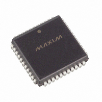
DS87C520-QNL+T&R Maxim Integrated Products, DS87C520-QNL+T&R Datasheet - Page 31

DS87C520-QNL+T&R
Manufacturer Part Number
DS87C520-QNL+T&R
Description
IC MCU EPROM/ROM 33MH IND 44PLCC
Manufacturer
Maxim Integrated Products
Series
87Cr
Datasheet
1.DS87C520-QCL.pdf
(43 pages)
Specifications of DS87C520-QNL+T&R
Core Processor
8051
Core Size
8-Bit
Speed
33MHz
Connectivity
EBI/EMI, SIO, UART/USART
Peripherals
Power-Fail Reset, WDT
Number Of I /o
32
Program Memory Size
16KB (16K x 8)
Program Memory Type
OTP
Ram Size
1K x 8
Voltage - Supply (vcc/vdd)
4.5 V ~ 5.5 V
Oscillator Type
External
Operating Temperature
-40°C ~ 85°C
Package / Case
44-LCC, 44-PLCC
Processor Series
DS87C520
Core
8051
Data Bus Width
8 bit
Data Ram Size
1 KB
Interface Type
UART
Maximum Clock Frequency
33 MHz
Number Of Programmable I/os
32
Number Of Timers
3
Operating Supply Voltage
4.5 V to 5.5 V
Maximum Operating Temperature
+ 85 C
Mounting Style
SMD/SMT
3rd Party Development Tools
PK51, CA51, A51, ULINK2
Minimum Operating Temperature
- 40 C
Package
44PLCC
Device Core
8051
Family Name
87C
Maximum Speed
33 MHz
Lead Free Status / RoHS Status
Lead free / RoHS Compliant
Eeprom Size
-
Data Converters
-
Lead Free Status / Rohs Status
Details
Note 1:
Note 2:
Note 3:
Note 4:
Note 5:
Note 6:
Note 7:
Note 8:
Note 9:
Note 10:
Note 11:
Note 12:
DC ELECTRICAL CHARACTERISTICS (continued)
(V
TYPICAL I
Transition Current from 1 to 0 Ports 1, 2, 3
at 2V
Input Leakage Port 0, and EA pins, I/O
Mode
Input Leakage Port 0, Bus Mode
RST Pulldown Resistance
CC
= 4.5V, T
Stop mode current measured with XTAL1 and RST grounded, V
When addressing external memory. This specification only applies to the first clock cycle following the transition.
RST = V
state during I/O mode.
During a 0-to-1 transition, a one-shot drives the ports hard for two clock cycles. This measurement reflects port in
transition mode.
Ports 1, 2, and 3 source transition current when being pulled down externally. It reaches its maximum at approximately
2V.
0.45 < V
occurs near the input transition point of the latch, approximately 2V.
0.45 < V
This is the current required from an external circuit to hold a logic low level on an I/O pin while the corresponding port
latch bit is set to 1. This is only the current required to hold the low level; transitions from 1 to 0 on an I/O pin will also
have to overcome the transition current.
All parameters apply to both commercial and industrial temperature operation, unless otherwise noted.
All voltages are referenced to ground.
Active current measured with 33MHz clock source on XTAL1, V
Idle mode current measured with 33MHz clock source on XTAL1, V
disconnected.
CC
PARAMETER
A
vs. FREQUENCY
= -40°C to +85°C.)
IN
IN
CC
< V
< V
. This condition mimics operation of pins in I/O mode. Port 0 is tri-stated in reset and when at a logic high
CC
CC
. Not a high-impedance input. This port is a weak address holding latch in Bus Mode. Peak current
. RST = V
CC
. This condition mimics operation of pins in I/O mode.
SYMBOL
DS87C520/DS83C520 EPROM/ROM High-Speed Microcontrollers
R
I
I
I
TL
RST
L
L
31 of 43
MIN
-300
-10
50
CC
CC
= RST = 5.5V, other pins disconnected.
= 5.5V, all other pins disconnected.
CC
= 5.5V, RST at ground, other pins
TYP
MAX
+300
-800
+10
200
UNITS
μA
μA
μA
k
NOTES
11
10
9


