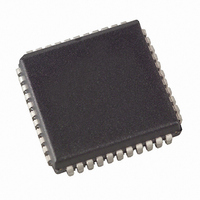
T89C51RD2-SLSIM Atmel, T89C51RD2-SLSIM Datasheet - Page 78

T89C51RD2-SLSIM
Manufacturer Part Number
T89C51RD2-SLSIM
Description
IC MICRO CTRL 64K FLASH 44PLCC
Manufacturer
Atmel
Series
89Cr
Datasheet
1.T89C51RD2-SMSIM.pdf
(104 pages)
Specifications of T89C51RD2-SLSIM
Core Processor
8051
Core Size
8-Bit
Speed
40MHz
Connectivity
SPI, UART/USART
Peripherals
POR, PWM, WDT
Number Of I /o
32
Program Memory Size
64KB (64K x 8)
Program Memory Type
FLASH
Eeprom Size
2K x 8
Ram Size
1.25K x 8
Voltage - Supply (vcc/vdd)
4.5 V ~ 5.5 V
Oscillator Type
Internal
Operating Temperature
-40°C ~ 85°C
Package / Case
44-PLCC
Lead Free Status / RoHS Status
Contains lead / RoHS non-compliant
Data Converters
-
Programming Algorithm
Verify Algorithm
78
T89C51RD2
To program the T89C51RD2 the following sequence must be exercised:
•
•
If the security bits are activated, the following commands must be done before
programming:
•
•
•
•
•
•
To write a page in the Flash memory, execute the following steps:
•
•
•
•
•
•
Repeat step 2 through 5 changing the address and data for end of a 128 bytes page
•
•
•
•
Repeat step 0 through 9 changing the address and data until the entire array or until the
end of the object file is reached (See Figure 32.)
•
Verify must be done after each byte or block of bytes is programmed. In either case, a
complete verify of the programmed array will ensure reliable programming of the
T89C51RD2.
P 2.7 is used to enable data output.
To verify the T89C51RD2 code the following sequence must be exercised:
•
•
•
Repeat step 2 through 3 changing the address for the entire array verification
(See Figure 32.).
Check the signature bytes
Check the HSB (VSB mode)
Unlock test modes (PEULCK mode, pulse 55h and AAh)
Chip erase (CERR mode)
Write FFh in the HSB (PGMS mode)
Write the signature bytes content in the XAF
As the boot loader and the XAF content is lost after a "chip erase", it must be
reprogrammed if needed.
Disable programming access (PELCK mode)
Step 0: Enable programming access (PEULCK mode)
Step 1: Activate the combination of control signals (PGML mode)
Step 2: Input the valid address on the address lines (High order bits of the address
must be stable during the complete ALE low time)
Step 3: Activate the combination of control signals (PGML mode)
Step 4: Input the appropriate data on the data lines.
Step 5: Pulse ALE/PROG once.
Step 6: Enable programming access (PEULCK mode)
Step 7: Activate the combination of control signals (PGMC mode)
Step 8: Input the valid address on the address lines.
Step 9: Pulse ALE/PROG once the specified write time is reached.
Step 10: Disable programming access (PELCK mode)
Step 1:Activate the combination of program and control signals (PGMV)
Step 2: Input the valid address on the address lines.
Step 3: Read data on the data lines.
4243G–8051–05/03


