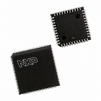
PXAG49KFA/00,512 NXP Semiconductors, PXAG49KFA/00,512 Datasheet - Page 10

PXAG49KFA/00,512
Manufacturer Part Number
PXAG49KFA/00,512
Description
IC XA MCU 16BIT FLASH 64K 44PLCC
Manufacturer
NXP Semiconductors
Series
XAr
Datasheet
1.PXAG49KBA00512.pdf
(42 pages)
Specifications of PXAG49KFA/00,512
Core Processor
XA
Core Size
16-Bit
Speed
30MHz
Connectivity
UART/USART
Peripherals
PWM, WDT
Number Of I /o
32
Program Memory Size
64KB (64K x 8)
Program Memory Type
FLASH
Ram Size
2K x 8
Voltage - Supply (vcc/vdd)
4.75 V ~ 5.25 V
Oscillator Type
External
Operating Temperature
-40°C ~ 85°C
Package / Case
44-PLCC
Lead Free Status / RoHS Status
Lead free / RoHS Compliant
Eeprom Size
-
Data Converters
-
Other names
568-1098-5
935267441512
PXAG49KFA
935267441512
PXAG49KFA
Available stocks
Company
Part Number
Manufacturer
Quantity
Price
Company:
Part Number:
PXAG49KFA/00,512
Manufacturer:
NXP Semiconductors
Quantity:
10 000
Philips Semiconductors
FLASH EPROM MEMORY
GENERAL DESCRIPTION
The XA-G49 Flash memory augments EPROM functionality with
in-circuit electrical erasure and programming. The Flash can be read
and written as bytes. The Chip Erase operation will erase the entire
program memory. The Block Erase function can erase any single
Flash block. In-circuit programming and standard parallel
programming are both available. On-chip erase and write timing
generation contribute to a user friendly programming interface.
The XA-G49 Flash reliably stores memory contents even after
10,000 erase and program cycles. The cell is designed to optimize
the erase and programming mechanisms. In addition, the
combination of advanced tunnel oxide processing and low internal
electric fields for erase and programming operations produces
reliable cycling. For In-System Programming, the XA-G49 can use a
single +5 V power supply. Faster In-System Programming may be
obtained, if required, through the use of a +12 V V
Parallel programming (using separate programming hardware) uses
a +12 V V
FEATURES
2001 Jun 27
programming routines and a default loader. The Boot ROM can be
Flash EPROM internal program memory with Single Voltage
Programming and Block Erase capability.
Internal 2 kbyte fixed boot ROM, containing low-level
turned off to provide access to the full 64 kbyte Flash memory.
Boot vector allows user provided Flash loader code to reside
anywhere in the Flash memory space. This configuration provides
flexibility to the user.
Default loader in Boot ROM allows programming via the serial port
without the need for a user provided loader.
Up to 1 Mbyte external program memory if the internal program
memory is disabled (EA = 0).
Programming and erase voltage: V
or 12 V 5% for In System Programming. Using 12 V V
improves programming and erase time.
Read/Programming/Erase in ISP:
– Byte-wise read (60 ns access time).
– Byte Programming (3–4 minutes for 64 K flash, depending on
In-circuit programming via user selected method, typically RS232
or parallel I/O port interface.
Programmable security for the code in the Flash.
10,000 minimum erase/program cycles each byte over operating
temperature range.
10 year minimum data retention.
XA 16-bit microcontroller family
64K Flash/2K RAM, watchdog, 2 UARTs
clock frequency).
PP
supply
PP
= V
DD
(5 V power supply),
PP
supply.
PP
for ISP
10
Programming of the Flash memory is accomplished one byte at a time.
CAPABILITIES OF THE PHILIPS XA-G49
FLASH-BASED MICROCONTROLLERS
Flash organization
The XA-G49 contains 64 kbytes of Flash program memory. This
memory is organized as 5 separate blocks. The first two blocks are
8 kbytes in size, filling the program memory space from address 0
through 3FFF hex. The final three blocks are 16 kbytes in size and
occupy addresses from 4000 through FFFF hex.
Figure 3 depicts the Flash memory configuration.
Flash Programming and Erasure
The XA-G49 Flash microcontroller supports a number of
programming possibilities for the on-chip Flash memory. The Flash
memory may be programmed in a parallel fashion on standard
programming equipment in a manner similar to an EPROM
microcontroller. The XA-G49 microcontroller is able to program its
own Flash memory while the application code is running. Also, a
default loader built into a Boot ROM allows programming blank
devices serially through the UART.
Using any of these types of programming, any of the individual blocks
may be erased separately, or the entire chip may be erased.
Boot ROM
When the microcontroller programs its own Flash memory, all of the
low level details are handled by code that is permanently contained
in a 2 kbyte “Boot ROM” that is separate from the Flash memory. A
user program simply calls the entry point with the appropriate
parameters to accomplish the desired operation. Boot ROM
operations include things like: erase block, program byte, verify
byte, program security lock bit, etc. The Boot ROM overlays the
program memory space at the top of the address space from F800
to FFFF hex, when it is enabled by setting the ENBOOT bit at
AUXR1.7.. The Boot ROM may be turned off so that the upper
2 kbytes of Flash program memory are accessible for execution.
ENBOOT and PWR_VLD
Setting the ENBOOT bit in the AUXR register enables the Boot
ROM and activates the on-chip V
V
V
should be checked prior to calling the Boot ROM for programming
and erase services. When ENBOOT is set, it typically takes
5 microseconds for the internal programming voltage to be ready.
The ENBOOT bit will automatically be set if the status byte is
non-zero during reset, or when PSEN is low, ALE is high, and EA is
high at the falling edge of reset. Otherwise, ENBOOT will be cleared
during reset.
When programming functions are not needed, ENBOOT may be
cleared. This enables access to the 2 kbytes of Flash code memory
that is overlaid by the Boot ROM, allowing a full 64 kbytes of Flash
code memory.
DD
PP
is available for programming and erase operations. This flag
rather than 12 V externally. The PWR_VLD flag indicates that
PP
generator if V
PP
XA-G49
Preliminary data
is connected to


