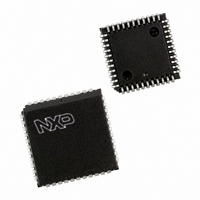
PXAG49KFA/00,512 NXP Semiconductors, PXAG49KFA/00,512 Datasheet - Page 8

PXAG49KFA/00,512
Manufacturer Part Number
PXAG49KFA/00,512
Description
IC XA MCU 16BIT FLASH 64K 44PLCC
Manufacturer
NXP Semiconductors
Series
XAr
Datasheet
1.PXAG49KBA00512.pdf
(42 pages)
Specifications of PXAG49KFA/00,512
Core Processor
XA
Core Size
16-Bit
Speed
30MHz
Connectivity
UART/USART
Peripherals
PWM, WDT
Number Of I /o
32
Program Memory Size
64KB (64K x 8)
Program Memory Type
FLASH
Ram Size
2K x 8
Voltage - Supply (vcc/vdd)
4.75 V ~ 5.25 V
Oscillator Type
External
Operating Temperature
-40°C ~ 85°C
Package / Case
44-PLCC
Lead Free Status / RoHS Status
Lead free / RoHS Compliant
Eeprom Size
-
Data Converters
-
Other names
568-1098-5
935267441512
PXAG49KFA
935267441512
PXAG49KFA
Available stocks
Company
Part Number
Manufacturer
Quantity
Price
Company:
Part Number:
PXAG49KFA/00,512
Manufacturer:
NXP Semiconductors
Quantity:
10 000
*
1. At reset, the BCR register is loaded with the binary value 0000 0a11, where “a” is the value on the BUSW pin. This defaults the address bus
2. SFR is loaded from the reset vector.
3. All bits except F1, F0, and P are loaded from the reset vector. Those bits are all 0.
4. Unimplemented bits in SFRs are X (unknown) at all times. Ones should not be written to these bits since they may be used for other
5. Port configurations default to quasi-bidirectional when the XA begins execution from internal code memory after reset, based on the
6. The WDCON reset value is E6 for a Watchdog reset, E4 for all other reset causes.
7. The XA-G49 implements an 8-bit SFR bus, as stated in Chapter 8 of the XA User Guide . All SFR accesses must be 8-bit operations. Attempts
8. The AUXR reset value is typically 00h. If the Boot Loader is activated at reset because the Flash status byte is non-zero or because the Boot
Philips Semiconductors
NOTES:
2001 Jun 27
SWR*
T2CON*
T2MOD*
TH2
TL2
T2CAPH
T2CAPL
TCON*
TH0
TH1
TL0
TL1
TMOD
TSTAT*
WDCON*
WDL
WFEED1
WFEED2
NAME
NAME
XA 16-bit microcontroller family
64K Flash/2K RAM, watchdog, 2 UARTs
SFRs are bit addressable.
size to 20 bits since the XA-G49 has only 20 address lines.
purposes in future XA derivatives. The reset value shown for these bits is 0.
condition found on the EA pin. Thus all PnCFGA registers will contain FF and PnCFGB registers will contain 00. When the XA begins
execution using external code memory, the default configuration for pins that are associated with the external bus will be push-pull. The
PnCFGA and PnCFGB register contents will reflect this difference.
to write 16 bits to an SFR will actually write only the lower 8 bits. Sixteen bit SFR reads will return undefined data in the upper byte.
Vector has been forced (by PSEN = 0, ALE = 1, EA = 1 at reset), the AUXR reset value will be 1x00 0000b. Bit 6 will be a 1 if the on-chip
V
PP
generator is running and ready, otherwise it will be a 0.
Software Interrupt Request
Timer 2 control register
Timer 2 mode control
Timer 2 high byte
Timer 2 low byte
Timer 2 capture register,
high byte
Timer 2 capture register,
low byte
Timer 0 and 1 control register
Timer 0 high byte
Timer 1 high byte
Timer 0 low byte
Timer 1 low byte
Timer 0 and 1 mode control
Timer 0 and 1 extended status
Watchdog control register
Watchdog timer reload
Watchdog feed 1
Watchdog feed 2
DESCRIPTION
DESCRIPTION
ADDRESS
ADDRESS
42A
45B
45A
45C
41F
45F
45D
45E
SFR
SFR
418
419
459
458
410
451
453
450
452
411
GATE
PRE2
MSB
2C7
2CF
357
TF2
287
TF1
28F
2FF
—
—
—
SWR7
EXF2
PRE1
2CE
TR1
2C6
28E
2FE
356
286
C/T
—
—
8
BIT FUNCTIONS AND ADDRESSES
RCLK0
RCLK1
SWR6
PRE0
2CD
2FD
2C5
TF0
28D
355
285
M1
—
TCLK0 EXEN2
TCLK1
SWR5
2CC
2C4
TR0
28C
2FC
354
284
M0
—
—
SWR4
GATE
2C3
2CB
2FB
353
283
28B
IE1
—
—
—
WDRUN
SWR3
T1OE
TR2
2CA
2C2
28A
2FA
352
282
C/T
IT1
—
WDTOF
SWR2
T2OE
C/T2
2C1
2C9
351
281
289
2F9
IE0
M1
—
CP/RL2
SWR1
DCEN
T0OE
XA-G49
LSB
2C0
2C8
350
280
288
2F8
IT0
Preliminary data
M0
—
RESET
RESET
VALUE
VALUE
Note 6
00
00
00
00
00
00
00
00
00
00
00
00
00
00
00
x
x


