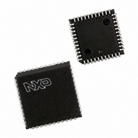
PXAG49KFA/00,512 NXP Semiconductors, PXAG49KFA/00,512 Datasheet - Page 6

PXAG49KFA/00,512
Manufacturer Part Number
PXAG49KFA/00,512
Description
IC XA MCU 16BIT FLASH 64K 44PLCC
Manufacturer
NXP Semiconductors
Series
XAr
Datasheet
1.PXAG49KBA00512.pdf
(42 pages)
Specifications of PXAG49KFA/00,512
Core Processor
XA
Core Size
16-Bit
Speed
30MHz
Connectivity
UART/USART
Peripherals
PWM, WDT
Number Of I /o
32
Program Memory Size
64KB (64K x 8)
Program Memory Type
FLASH
Ram Size
2K x 8
Voltage - Supply (vcc/vdd)
4.75 V ~ 5.25 V
Oscillator Type
External
Operating Temperature
-40°C ~ 85°C
Package / Case
44-PLCC
Lead Free Status / RoHS Status
Lead free / RoHS Compliant
Eeprom Size
-
Data Converters
-
Other names
568-1098-5
935267441512
PXAG49KFA
935267441512
PXAG49KFA
Available stocks
Company
Part Number
Manufacturer
Quantity
Price
Company:
Part Number:
PXAG49KFA/00,512
Manufacturer:
NXP Semiconductors
Quantity:
10 000
Philips Semiconductors
SPECIAL FUNCTION REGISTERS
2001 Jun 27
MNEMONIC
MNEMONIC
AUXR
BCR
BTRH
BTRL
CS
DS
ES
IEH*
IEL*
IPA0
IPA1
IPA2
IPA4
IPA5
P0*
P1*
P2*
P3*
EA/WAIT/
NAME
NAME
XA 16-bit microcontroller family
64K Flash/2K RAM, watchdog, 2 UARTs
XTAL1
XTAL2
PSEN
V
PP
Auxiliary function register
Bus configuration register
Bus timing register high byte
Bus timing register low byte
Code segment
Data segment
Extra segment
Interrupt enable high byte
Interrupt enable low byte
Interrupt priority 0
Interrupt priority 1
Interrupt priority 2
Interrupt priority 4
Interrupt priority 5
Port 0
Port 1
Port 2
Port 3
LCC
32
35
21
20
PIN. NO.
DESCRIPTION
DESCRIPTION
LQFP
26
29
15
14
TYPE
TYPE
O
O
I
I
Program Store Enable: The read strobe for external program memory. When the microcontroller
accesses external program memory, PSEN is driven low in order to enable memory devices. PSEN
is only active when external code accesses are performed.
External Access/Wait/Programming Supply Voltage: The EA input determines whether the
internal program memory of the microcontroller is used for code execution. The value on the EA pin
is latched as the external reset input is released and applies during later execution. When latched
as a 0, external program memory is used exclusively, when latched as a 1, internal program
memory will be used up to its limit, and external program memory used above that point. After reset
is released, this pin takes on the function of bus Wait input. If Wait is asserted high during any
external bus access, that cycle will be extended until Wait is released. During EPROM
programming, this pin is also the programming supply voltage input.
Crystal 1: Input to the inverting amplifier used in the oscillator circuit and input to the internal clock
generator circuits.
Crystal 2: Output from the oscillator amplifier.
ADDRESS
ADDRESS
44C
46A
4A0
4A1
4A2
4A4
4A5
SFR
SFR
469
468
443
441
442
427
426
430
431
432
433
ENBOOT
T2EX
WM1
MSB
DW1
P2.7
AD7
33F
337
387
38F
397
39F
EA
RD
—
—
—
—
—
—
—
FMIDLE
WM0
DW0
P2.6
AD6
33E
38E
39E
336
386
396
WR
T2
—
—
—
6
BIT FUNCTIONS AND ADDRESSES
PWR_VLD
DWA1
ALEW
TxD1
PTI0
PTI1
P2.5
AD5
33D
PT0
PT1
38D
39D
335
385
395
T1
—
—
—
—
NAME AND FUNCTION
NAME AND FUNCTION
WAITD
DWA0
RxD1
P2.4
33C
ET2
AD4
38C
39C
334
384
394
T0
—
—
—
BUSD
INT1
DR1
CR1
ETI1
P2.3
ET1
AD3
33B
333
383
38B
393
39B
A3
—
—
—
—
—
—
ERI1
INT0
P2.2
BC2
DR0
CR0
EX1
AD2
33A
38A
39A
332
382
392
A2
—
DRA1
CRA1
TxD0
PRI0
PRI1
ETI0
P2.1
BC1
PX0
PX1
AD1
ET0
PT2
339
331
381
389
391
399
A1
—
DRA0
CRA0
RxD0
WRH
XA-G49
ERI0
LSB
BC0
AD0
P2.0
EX0
338
330
380
388
390
398
Preliminary data
—
RESET
VALUE
Note 1
FF
EF
FF
FF
FF
FF
00
00
00
00
00
00
00
00
00
00


