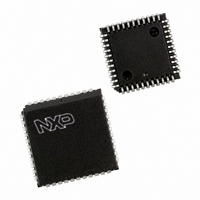
PXAG49KFA/00,512 NXP Semiconductors, PXAG49KFA/00,512 Datasheet - Page 22

PXAG49KFA/00,512
Manufacturer Part Number
PXAG49KFA/00,512
Description
IC XA MCU 16BIT FLASH 64K 44PLCC
Manufacturer
NXP Semiconductors
Series
XAr
Datasheet
1.PXAG49KBA00512.pdf
(42 pages)
Specifications of PXAG49KFA/00,512
Core Processor
XA
Core Size
16-Bit
Speed
30MHz
Connectivity
UART/USART
Peripherals
PWM, WDT
Number Of I /o
32
Program Memory Size
64KB (64K x 8)
Program Memory Type
FLASH
Ram Size
2K x 8
Voltage - Supply (vcc/vdd)
4.75 V ~ 5.25 V
Oscillator Type
External
Operating Temperature
-40°C ~ 85°C
Package / Case
44-PLCC
Lead Free Status / RoHS Status
Lead free / RoHS Compliant
Eeprom Size
-
Data Converters
-
Other names
568-1098-5
935267441512
PXAG49KFA
935267441512
PXAG49KFA
Available stocks
Company
Part Number
Manufacturer
Quantity
Price
Company:
Part Number:
PXAG49KFA/00,512
Manufacturer:
NXP Semiconductors
Quantity:
10 000
Philips Semiconductors
timer register is loaded with FFFF hex. The underflow also sets the
TF2 flag, which can generate an interrupt if enabled.
The external flag EXF2 toggles when Timer 2 underflows or
overflows. This EXF2 bit can be used as a 17th bit of resolution, if
needed. the EXF2 flag does not generate an interrupt in this mode.
As the baud rate generator, timer T2 is incremented by TCLK.
Baud Rate Generator Mode
By setting the TCLKn and/or RCLKn in T2CON or T2MOD, the
Timer 2 can be chosen as the baud rate generator for either or both
UARTs. The baud rates for transmit and receive can be
simultaneously different.
Programmable Clock-Out
A 50% duty cycle clock can be programmed to come out on P1.6.
This pin, besides being a regular I/O pin, has two alternate
functions. It can be programmed (1) to input the external clock for
Table 4. Timer 2 Operating Modes
2001 Jun 27
XA 16-bit microcontroller family
64K Flash/2K RAM, watchdog, 2 UARTs
TSTAT
Bit Addressable
Reset Value: 00H
T2MOD
Bit Addressable
Reset Value: 00H
TR2
0
1
1
1
1
BIT
TSTAT.2
TSTAT.0
BIT
T2MOD.5 RCLK1
T2MOD.4 TCLK1
T2MOD.1 T2OE
T2MOD.0 DCEN
Address:411
Address:419
CP/RL2
SYMBOL FUNCTION
SYMBOL
T1OE
T0OE
X
0
0
1
X
Receive Clock Flag.
Transmit Clock Flag. RCLK1 and TCLK1 are used to select Timer 2 overflow rate as a clock source
for UART1 instead of Timer T1.
When 0, this bit allows the T2 pin to clock Timer 2 when in the counter mode.
When 1, T2 acts as an output and toggles at every Timer 2 overflow.
Controls count direction for Timer 2 in autoreload mode.
DCEN=0 counter set to count up only
DCEN=1 counter set to count up or down, depending on T2EX (see text).
RCLK+TCLK
FUNCTION
When 0, this bit allows the T1 pin to clock Timer 1 when in the counter mode.
When 1, T1 acts as an output and toggles at every Timer 1 overflow.
When 0, this bit allows the T0 pin to clock Timer 0 when in the counter mode.
When 1, T0 acts as an output and toggles at every Timer 0 overflow.
X
0
0
0
1
MSB
MSB
Figure 9. Timer 0 And 1 Extended Status (TSTAT)
—
—
Figure 10. Timer 2 Mode Control (T2MOD)
—
—
DCEN
X
X
X
0
1
RCLK1
—
22
TCLK1
16-bit auto-reload, counting up or down depending on T2EX pin
—
Timer/Counter 2 or (2) to output a 50% duty cycle clock ranging from
3.58Hz to 3.75MHz at a 30MHz operating frequency.
To configure the Timer/Counter 2 as a clock generator, bit C/T2 (in
T2CON) must be cleared and bit T20E in T2MOD must be set. Bit
TR2 (T2CON.2) also must be set to start the timer.
The Clock-Out frequency depends on the oscillator frequency and
the reload value of Timer 2 capture registers (TCAP2H, TCAP2L) as
shown in this equation:
In the Clock-Out mode Timer 2 roll-overs will not generate an
interrupt. This is similar to when it is used as a baud-rate generator.
It is possible to use Timer 2 as a baud-rate generator and a clock
generator simultaneously. Note, however, that the baud-rate will be
1/8 of the Clock-Out frequency.
—
—
2
(65536 * TCAP2H, TCAP2L)
16-bit auto-reload, counting up
T1OE
—
Baud rate generator
Timer off (stopped)
16-bit capture
TCLK
MODE
T2OE
—
DCEN
T0OE
SU00612B
LSB
LSB
SU00610B
XA-G49
Preliminary data


