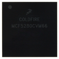
MCF5280CVM66 Freescale Semiconductor, MCF5280CVM66 Datasheet - Page 229

MCF5280CVM66
Manufacturer Part Number
MCF5280CVM66
Description
IC MPU 32BIT COLDF 256-MAPBGA
Manufacturer
Freescale Semiconductor
Series
MCF528xr
Datasheet
1.MCF5216CVM66J.pdf
(766 pages)
Specifications of MCF5280CVM66
Core Processor
Coldfire V2
Core Size
32-Bit
Speed
66MHz
Connectivity
CAN, EBI/EMI, Ethernet, I²C, SPI, UART/USART
Peripherals
DMA, LVD, POR, PWM, WDT
Number Of I /o
142
Program Memory Type
ROMless
Ram Size
64K x 8
Voltage - Supply (vcc/vdd)
2.7 V ~ 3.6 V
Data Converters
A/D 8x10b
Oscillator Type
External
Operating Temperature
-40°C ~ 85°C
Package / Case
256-MAPBGA
Controller Family/series
ColdFire
No. Of I/o's
150
Program Memory Size
2KB
Ram Memory Size
64KB
Cpu Speed
66.67MHz
Embedded Interface Type
CAN, I2C, SPI, UART
No. Of Pwm Channels
8
Rohs Compliant
Yes
Lead Free Status / RoHS Status
Lead free / RoHS Compliant
Eeprom Size
-
Program Memory Size
-
Available stocks
Company
Part Number
Manufacturer
Quantity
Price
Company:
Part Number:
MCF5280CVM66
Manufacturer:
FREESCAL
Quantity:
151
Company:
Part Number:
MCF5280CVM66
Manufacturer:
Freescale Semiconductor
Quantity:
10 000
Company:
Part Number:
MCF5280CVM66J
Manufacturer:
Freescale Semiconductor
Quantity:
10 000
Company:
Part Number:
MCF5280CVM66L
Manufacturer:
FREESCAL
Quantity:
151
- Current page: 229 of 766
- Download datasheet (9Mb)
Table 13-3
Freescale Semiconductor
S0
S1
S2
S3
S4
State
describes the states as they appear in subsequent timing diagrams.
All
All
Fast
Termination
Read/write
(skipped fast
termination)
Write
Read/write
(skipped for
fast
termination)
Read
All
Read
(including
fast-terminati
on)
Cycle
High
Low
High
Low
High
CLKOUT
MCF5282 and MCF5216 ColdFire Microcontroller User’s Manual, Rev. 3
Figure 13-4. Data Transfer State Transition Diagram
Next Cycle
S5
S4
The read or write cycle is initiated in S0. On the rising edge of CLKOUT, the device
places a valid address on the address bus and drives R/W high for a read and low
for a write, if it is not already in the appropriate state. The processor asserts TIP,
SIZ[1:0], and TS on the rising edge of CLKOUT.
The appropriate CSn, BS, and OE signals assert on the CLKOUT falling edge.
TA must be asserted during S1. Data is made available by the external device and
is sampled on the rising edge of CLKOUT with TA asserted.
TS is negated on the rising edge of CLKOUT in S2.
The data bus is driven out of high impedance as data is placed on the bus on the
rising edge of CLKOUT.
The processor waits for TA assertion. If TA is not sampled as asserted before the
rising edge of CLKOUT at the end of the first clock cycle, the processor inserts wait
states (full clock cycles) until TA is sampled as asserted.
Data is made available by the external device on the falling edge of CLKOUT and
is sampled on the rising edge of CLKOUT with TA asserted.
The external device should negate TA.
The external device can stop driving data after the rising edge of CLKOUT.
However data could be driven through the end of S5.
Table 13-3. Bus Cycle States
Termination
Fast
S0
S3
Wait
States
Description
S1
S2
Basic
Read/Write
External Interface Module (EIM)
13-5
Related parts for MCF5280CVM66
Image
Part Number
Description
Manufacturer
Datasheet
Request
R
Part Number:
Description:
Manufacturer:
Freescale Semiconductor, Inc
Datasheet:
Part Number:
Description:
Manufacturer:
Freescale Semiconductor, Inc
Datasheet:
Part Number:
Description:
Manufacturer:
Freescale Semiconductor, Inc
Datasheet:
Part Number:
Description:
Manufacturer:
Freescale Semiconductor, Inc
Datasheet:
Part Number:
Description:
Manufacturer:
Freescale Semiconductor, Inc
Datasheet:
Part Number:
Description:
Manufacturer:
Freescale Semiconductor, Inc
Datasheet:
Part Number:
Description:
Manufacturer:
Freescale Semiconductor, Inc
Datasheet:
Part Number:
Description:
Manufacturer:
Freescale Semiconductor, Inc
Datasheet:
Part Number:
Description:
Manufacturer:
Freescale Semiconductor, Inc
Datasheet:
Part Number:
Description:
Manufacturer:
Freescale Semiconductor, Inc
Datasheet:
Part Number:
Description:
Manufacturer:
Freescale Semiconductor, Inc
Datasheet:
Part Number:
Description:
Manufacturer:
Freescale Semiconductor, Inc
Datasheet:
Part Number:
Description:
Manufacturer:
Freescale Semiconductor, Inc
Datasheet:
Part Number:
Description:
Manufacturer:
Freescale Semiconductor, Inc
Datasheet:
Part Number:
Description:
Manufacturer:
Freescale Semiconductor, Inc
Datasheet:


