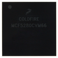
MCF5280CVM66 Freescale Semiconductor, MCF5280CVM66 Datasheet - Page 695

MCF5280CVM66
Manufacturer Part Number
MCF5280CVM66
Description
IC MPU 32BIT COLDF 256-MAPBGA
Manufacturer
Freescale Semiconductor
Series
MCF528xr
Datasheet
1.MCF5216CVM66J.pdf
(766 pages)
Specifications of MCF5280CVM66
Core Processor
Coldfire V2
Core Size
32-Bit
Speed
66MHz
Connectivity
CAN, EBI/EMI, Ethernet, I²C, SPI, UART/USART
Peripherals
DMA, LVD, POR, PWM, WDT
Number Of I /o
142
Program Memory Type
ROMless
Ram Size
64K x 8
Voltage - Supply (vcc/vdd)
2.7 V ~ 3.6 V
Data Converters
A/D 8x10b
Oscillator Type
External
Operating Temperature
-40°C ~ 85°C
Package / Case
256-MAPBGA
Controller Family/series
ColdFire
No. Of I/o's
150
Program Memory Size
2KB
Ram Memory Size
64KB
Cpu Speed
66.67MHz
Embedded Interface Type
CAN, I2C, SPI, UART
No. Of Pwm Channels
8
Rohs Compliant
Yes
Lead Free Status / RoHS Status
Lead free / RoHS Compliant
Eeprom Size
-
Program Memory Size
-
Available stocks
Company
Part Number
Manufacturer
Quantity
Price
Company:
Part Number:
MCF5280CVM66
Manufacturer:
FREESCAL
Quantity:
151
Company:
Part Number:
MCF5280CVM66
Manufacturer:
Freescale Semiconductor
Quantity:
10 000
Company:
Part Number:
MCF5280CVM66J
Manufacturer:
Freescale Semiconductor
Quantity:
10 000
Company:
Part Number:
MCF5280CVM66L
Manufacturer:
FREESCAL
Quantity:
151
- Current page: 695 of 766
- Download datasheet (9Mb)
33.8
Table 33-14
Timings listed in
Freescale Semiconductor
1
2
3
1
2
Maximum number of guaranteed program/erase cycles
Data retention at average operating temperature of 85°C
Name
B1a
B1b
B2a
B2b
Timing specifications have been indicated taking into account the full drive strength for the pads.
TEA and TA pins are being referred to as control inputs.
B0
B4
B5
A program/erase cycle is defined as switching the bits from 1 → 0 → 1.
Reprogramming of a Flash array block prior to erase is not required.
Refer to figure A-19.
External Interface Timing Characteristics
CLKOUT — MCF521x
CLKOUT — MCF528x
Control input valid to CLKOUT high
BKPT valid to CLKOUT high
CLKOUT high to control inputs invalid
CLKOUT high to asynchronous control input BKPT invalid
Data input (D[31:0]) valid to CLKOUT high
CLKOUT high to data input (D[31:0]) invalid
lists processor bus input timings.
All processor bus timings are synchronous; that is, input setup/hold and
output delay with respect to the rising edge of a reference clock. The
reference clock is the CLKOUT output.
All other timing relationships can be derived from these values.
Table 33-14
MCF5282 and MCF5216 ColdFire Microcontroller User’s Manual, Rev. 3
Table 33-14. Processor Bus Input Timing Specifications
Table 33-13. SGFM Flash Module Life Characteristics
Parameter
are shown in
3
Characteristic
2
2
Figure
(V
DDF
Control Inputs
Data Inputs
1
NOTE
= 2.7 to 3.6 V)
1
33-2.
before failure
3
Retention
Symbol
P/E
Symbol
t
t
t
t
BKVCH
t
BKNCH
t
DIVCH
t
CVCH
CHCII
CHDII
CYC
10,000
Value
15.15
Electrical Characteristics
12.5
Min
10
10
10
0
0
6
0
2
Max
—
—
—
—
—
—
—
Cycles
Years
Unit
Unit
ns
ns
ns
ns
ns
ns
ns
33-11
Related parts for MCF5280CVM66
Image
Part Number
Description
Manufacturer
Datasheet
Request
R
Part Number:
Description:
Manufacturer:
Freescale Semiconductor, Inc
Datasheet:
Part Number:
Description:
Manufacturer:
Freescale Semiconductor, Inc
Datasheet:
Part Number:
Description:
Manufacturer:
Freescale Semiconductor, Inc
Datasheet:
Part Number:
Description:
Manufacturer:
Freescale Semiconductor, Inc
Datasheet:
Part Number:
Description:
Manufacturer:
Freescale Semiconductor, Inc
Datasheet:
Part Number:
Description:
Manufacturer:
Freescale Semiconductor, Inc
Datasheet:
Part Number:
Description:
Manufacturer:
Freescale Semiconductor, Inc
Datasheet:
Part Number:
Description:
Manufacturer:
Freescale Semiconductor, Inc
Datasheet:
Part Number:
Description:
Manufacturer:
Freescale Semiconductor, Inc
Datasheet:
Part Number:
Description:
Manufacturer:
Freescale Semiconductor, Inc
Datasheet:
Part Number:
Description:
Manufacturer:
Freescale Semiconductor, Inc
Datasheet:
Part Number:
Description:
Manufacturer:
Freescale Semiconductor, Inc
Datasheet:
Part Number:
Description:
Manufacturer:
Freescale Semiconductor, Inc
Datasheet:
Part Number:
Description:
Manufacturer:
Freescale Semiconductor, Inc
Datasheet:
Part Number:
Description:
Manufacturer:
Freescale Semiconductor, Inc
Datasheet:


