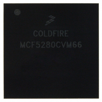
MCF5280CVM66 Freescale Semiconductor, MCF5280CVM66 Datasheet - Page 267

MCF5280CVM66
Manufacturer Part Number
MCF5280CVM66
Description
IC MPU 32BIT COLDF 256-MAPBGA
Manufacturer
Freescale Semiconductor
Series
MCF528xr
Datasheet
1.MCF5216CVM66J.pdf
(766 pages)
Specifications of MCF5280CVM66
Core Processor
Coldfire V2
Core Size
32-Bit
Speed
66MHz
Connectivity
CAN, EBI/EMI, Ethernet, I²C, SPI, UART/USART
Peripherals
DMA, LVD, POR, PWM, WDT
Number Of I /o
142
Program Memory Type
ROMless
Ram Size
64K x 8
Voltage - Supply (vcc/vdd)
2.7 V ~ 3.6 V
Data Converters
A/D 8x10b
Oscillator Type
External
Operating Temperature
-40°C ~ 85°C
Package / Case
256-MAPBGA
Controller Family/series
ColdFire
No. Of I/o's
150
Program Memory Size
2KB
Ram Memory Size
64KB
Cpu Speed
66.67MHz
Embedded Interface Type
CAN, I2C, SPI, UART
No. Of Pwm Channels
8
Rohs Compliant
Yes
Lead Free Status / RoHS Status
Lead free / RoHS Compliant
Eeprom Size
-
Program Memory Size
-
Available stocks
Company
Part Number
Manufacturer
Quantity
Price
Company:
Part Number:
MCF5280CVM66
Manufacturer:
FREESCAL
Quantity:
151
Company:
Part Number:
MCF5280CVM66
Manufacturer:
Freescale Semiconductor
Quantity:
10 000
Company:
Part Number:
MCF5280CVM66J
Manufacturer:
Freescale Semiconductor
Quantity:
10 000
Company:
Part Number:
MCF5280CVM66L
Manufacturer:
FREESCAL
Quantity:
151
- Current page: 267 of 766
- Download datasheet (9Mb)
Signal Descriptions
14.2.10.4 Request-to-Send (URTS[1:0])
The URTS[1:0] signals are automatic request to send outputs from the UART modules. URTS[1:0] can
also be configured to be asserted and negated as a function of the Rx FIFO level.
The URTS[1:0] outputs are each offered as secondary functions on four pins: DTIN3, DTOUT3, DTIN1
and DTOUT1.
14.2.11 General Purpose Timer Signals
These pins provide the external interface to the general purpose timer functions.
14.2.11.1 GPTA[3:0]
These pins provide the external interface to the timer A functions.
These pins can also be configured as GPIO PTA[3:0].
14.2.11.2 GPTB[3:0]
These pins provide the external interface to the timer B functions.
These pins can also be configured as GPIO PTB[3:0].
14.2.11.3 External Clock Input (SYNCA/SYNCB)
These pins are used to clear the clock for each of the two timers, and are provided as a means of
synchronization to externally clocked or timed events.
14.2.12 DMA Timer Signals
This section describes the signals of the four DMA timer modules.
14.2.12.1 DMA Timer 0 Input (DTIN0)
The DMA timer 0 input (DTIN0) can be programmed to cause events to occur in DMA timer 0. It can
either clock the event counter or provide a trigger to the timer value capture logic.
This pin can also be configured as GPIO PTD1, secondary function UCTS1, or secondary function
UCTS0.
14.2.12.2 DMA Timer 0 Output (DTOUT0)
The programmable DMA timer output (DTOUT0) pulse or toggle on various timer events.
This pin can also be configured as GPIO PTD0, secondary function UCTS1, or secondary function
UCTS0.
14.2.12.3 DMA Timer 1 Input (DTIN1)
The DMA timer 1 input (DTIN1) can be programmed to cause events to occur in DMA timer 1. This can
either clock the event counter or provide a trigger to the timer value capture logic.
MCF5282 and MCF5216 ColdFire Microcontroller User’s Manual, Rev. 3
Freescale Semiconductor
14-27
Related parts for MCF5280CVM66
Image
Part Number
Description
Manufacturer
Datasheet
Request
R
Part Number:
Description:
Manufacturer:
Freescale Semiconductor, Inc
Datasheet:
Part Number:
Description:
Manufacturer:
Freescale Semiconductor, Inc
Datasheet:
Part Number:
Description:
Manufacturer:
Freescale Semiconductor, Inc
Datasheet:
Part Number:
Description:
Manufacturer:
Freescale Semiconductor, Inc
Datasheet:
Part Number:
Description:
Manufacturer:
Freescale Semiconductor, Inc
Datasheet:
Part Number:
Description:
Manufacturer:
Freescale Semiconductor, Inc
Datasheet:
Part Number:
Description:
Manufacturer:
Freescale Semiconductor, Inc
Datasheet:
Part Number:
Description:
Manufacturer:
Freescale Semiconductor, Inc
Datasheet:
Part Number:
Description:
Manufacturer:
Freescale Semiconductor, Inc
Datasheet:
Part Number:
Description:
Manufacturer:
Freescale Semiconductor, Inc
Datasheet:
Part Number:
Description:
Manufacturer:
Freescale Semiconductor, Inc
Datasheet:
Part Number:
Description:
Manufacturer:
Freescale Semiconductor, Inc
Datasheet:
Part Number:
Description:
Manufacturer:
Freescale Semiconductor, Inc
Datasheet:
Part Number:
Description:
Manufacturer:
Freescale Semiconductor, Inc
Datasheet:
Part Number:
Description:
Manufacturer:
Freescale Semiconductor, Inc
Datasheet:


