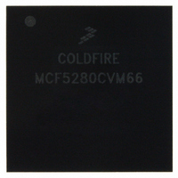
MCF5280CVM66 Freescale Semiconductor, MCF5280CVM66 Datasheet - Page 57

MCF5280CVM66
Manufacturer Part Number
MCF5280CVM66
Description
IC MPU 32BIT COLDF 256-MAPBGA
Manufacturer
Freescale Semiconductor
Series
MCF528xr
Datasheet
1.MCF5216CVM66J.pdf
(766 pages)
Specifications of MCF5280CVM66
Core Processor
Coldfire V2
Core Size
32-Bit
Speed
66MHz
Connectivity
CAN, EBI/EMI, Ethernet, I²C, SPI, UART/USART
Peripherals
DMA, LVD, POR, PWM, WDT
Number Of I /o
142
Program Memory Type
ROMless
Ram Size
64K x 8
Voltage - Supply (vcc/vdd)
2.7 V ~ 3.6 V
Data Converters
A/D 8x10b
Oscillator Type
External
Operating Temperature
-40°C ~ 85°C
Package / Case
256-MAPBGA
Controller Family/series
ColdFire
No. Of I/o's
150
Program Memory Size
2KB
Ram Memory Size
64KB
Cpu Speed
66.67MHz
Embedded Interface Type
CAN, I2C, SPI, UART
No. Of Pwm Channels
8
Rohs Compliant
Yes
Lead Free Status / RoHS Status
Lead free / RoHS Compliant
Eeprom Size
-
Program Memory Size
-
Available stocks
Company
Part Number
Manufacturer
Quantity
Price
Company:
Part Number:
MCF5280CVM66
Manufacturer:
FREESCAL
Quantity:
151
Company:
Part Number:
MCF5280CVM66
Manufacturer:
Freescale Semiconductor
Quantity:
10 000
Company:
Part Number:
MCF5280CVM66J
Manufacturer:
Freescale Semiconductor
Quantity:
10 000
Company:
Part Number:
MCF5280CVM66L
Manufacturer:
FREESCAL
Quantity:
151
- Current page: 57 of 766
- Download datasheet (9Mb)
instruction execution is performed in the second stage (EX) in one of the execute engines (e.g., ALU,
barrel shifter, divider, EMAC). There are no operand memory accesses associated with this class of
instructions, and the execution time is typically a single machine cycle. See
For memory-to-register (embedded-load) instructions, the instruction is effectively staged through the
OEP twice with a basic execution time of three cycles. First, the instruction is decoded and the components
of the operand address (base register from the RGF and displacement) are selected (DS). Second, the
operand effective address is generated using the ALU execute engine (AG). Third, the memory read
operand is fetched from the core bus, while any required register operand is simultaneously fetched (OC)
from the RGF. Finally, in the fourth cycle, the instruction is executed (EX). The heavily-used 32-bit load
instruction (
in
added to a base register Ay.
Freescale Semiconductor
Figure 2-12
Extension 1
Extension 2
Read Data
Core Bus
Opword
move.l <mem>y,Rx
shows an effective address of the form <ea>y = (d16,Ay), i.e., a 16-bit signed displacement
MCF5282 and MCF5216 ColdFire Microcontroller User’s Manual, Rev. 3
RGF
) is optimized to support a two-cycle execution time. The following example
Figure 2-11. V2 OEP Register-to-Register
Ry
DSOC
Operand Execution Pipeline
Rx
AGEX
new Rx
Figure
2-11.
Core Bus
Address
Core Bus
Write
Data
ColdFire Core
2-11
Related parts for MCF5280CVM66
Image
Part Number
Description
Manufacturer
Datasheet
Request
R
Part Number:
Description:
Manufacturer:
Freescale Semiconductor, Inc
Datasheet:
Part Number:
Description:
Manufacturer:
Freescale Semiconductor, Inc
Datasheet:
Part Number:
Description:
Manufacturer:
Freescale Semiconductor, Inc
Datasheet:
Part Number:
Description:
Manufacturer:
Freescale Semiconductor, Inc
Datasheet:
Part Number:
Description:
Manufacturer:
Freescale Semiconductor, Inc
Datasheet:
Part Number:
Description:
Manufacturer:
Freescale Semiconductor, Inc
Datasheet:
Part Number:
Description:
Manufacturer:
Freescale Semiconductor, Inc
Datasheet:
Part Number:
Description:
Manufacturer:
Freescale Semiconductor, Inc
Datasheet:
Part Number:
Description:
Manufacturer:
Freescale Semiconductor, Inc
Datasheet:
Part Number:
Description:
Manufacturer:
Freescale Semiconductor, Inc
Datasheet:
Part Number:
Description:
Manufacturer:
Freescale Semiconductor, Inc
Datasheet:
Part Number:
Description:
Manufacturer:
Freescale Semiconductor, Inc
Datasheet:
Part Number:
Description:
Manufacturer:
Freescale Semiconductor, Inc
Datasheet:
Part Number:
Description:
Manufacturer:
Freescale Semiconductor, Inc
Datasheet:
Part Number:
Description:
Manufacturer:
Freescale Semiconductor, Inc
Datasheet:


