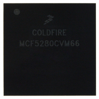
MCF5280CVM66 Freescale Semiconductor, MCF5280CVM66 Datasheet - Page 378

MCF5280CVM66
Manufacturer Part Number
MCF5280CVM66
Description
IC MPU 32BIT COLDF 256-MAPBGA
Manufacturer
Freescale Semiconductor
Series
MCF528xr
Datasheet
1.MCF5216CVM66J.pdf
(766 pages)
Specifications of MCF5280CVM66
Core Processor
Coldfire V2
Core Size
32-Bit
Speed
66MHz
Connectivity
CAN, EBI/EMI, Ethernet, I²C, SPI, UART/USART
Peripherals
DMA, LVD, POR, PWM, WDT
Number Of I /o
142
Program Memory Type
ROMless
Ram Size
64K x 8
Voltage - Supply (vcc/vdd)
2.7 V ~ 3.6 V
Data Converters
A/D 8x10b
Oscillator Type
External
Operating Temperature
-40°C ~ 85°C
Package / Case
256-MAPBGA
Controller Family/series
ColdFire
No. Of I/o's
150
Program Memory Size
2KB
Ram Memory Size
64KB
Cpu Speed
66.67MHz
Embedded Interface Type
CAN, I2C, SPI, UART
No. Of Pwm Channels
8
Rohs Compliant
Yes
Lead Free Status / RoHS Status
Lead free / RoHS Compliant
Eeprom Size
-
Program Memory Size
-
Available stocks
Company
Part Number
Manufacturer
Quantity
Price
Company:
Part Number:
MCF5280CVM66
Manufacturer:
FREESCAL
Quantity:
151
Company:
Part Number:
MCF5280CVM66
Manufacturer:
Freescale Semiconductor
Quantity:
10 000
Company:
Part Number:
MCF5280CVM66J
Manufacturer:
Freescale Semiconductor
Quantity:
10 000
Company:
Part Number:
MCF5280CVM66L
Manufacturer:
FREESCAL
Quantity:
151
- Current page: 378 of 766
- Download datasheet (9Mb)
General Purpose Timer Modules (GPTA and GPTB)
20.5.9
20.5.10 GPT Interrupt Enable Register (GPTIE)
20-10
Bit(s)
Bit(s)
7–0
7–0
GPT Control Register 2 (GPTCTL2)
Address
Address
Reset
Reset
Field
Field
EDGn[B:A]
R/W
R/W
OMx/OLx
Name
Name
EDG3B
MCF5282 and MCF5216 ColdFire Microcontroller User’s Manual, Rev. 3
7
7
Figure 20-12. GPT Interrupt Enable Register (GPTIE)
Figure 20-11. GPT Control Register 2 (GPTCTL2)
Output mode/output level. Selects the output action to be taken as a result of a
successful output compare on each channel. When either OMn or OLn is set and the
IOSn bit is set, the pin is an output regardless of the state of the corresponding DDR
bit. These bits are read anytime, write anytime.
00 GPT disconnected from output pin logic
01 Toggle OCn output line
10 Clear OCn output line
11 Set OCn line
Note: Channel 3 shares a pin with the pulse accumulator input pin. To use the PAI
input, clear both the OM3 and OL3 bits and clear the OC3M3 bit in the output compare
3 mask register.
Input capture edge control. Configures the input capture edge detector circuits for
each channel. These bits are read anytime, write anytime.
00 Input capture disabled
01 Input capture on rising edges only
10 Input capture on falling edges only
11 Input capture on any edge (rising or falling)
Table 20-12. GPTLCTL2 Field Descriptions
Table 20-11. GPTCL1 Field Descriptions
EDG3A EDG2B EDG2A EDG1B EDG1A EDG0B
6
6
—
IPSBAR + 0x1A_000C, 0x1B_000C
IPSBAR + 0x1A_000B, 0x1B_000B
5
5
0000_0000
0000_0000
4
4
R/W
R/W
Description
3
Description
3
2
CI
1
EDG0A
Freescale Semiconductor
0
0
Related parts for MCF5280CVM66
Image
Part Number
Description
Manufacturer
Datasheet
Request
R
Part Number:
Description:
Manufacturer:
Freescale Semiconductor, Inc
Datasheet:
Part Number:
Description:
Manufacturer:
Freescale Semiconductor, Inc
Datasheet:
Part Number:
Description:
Manufacturer:
Freescale Semiconductor, Inc
Datasheet:
Part Number:
Description:
Manufacturer:
Freescale Semiconductor, Inc
Datasheet:
Part Number:
Description:
Manufacturer:
Freescale Semiconductor, Inc
Datasheet:
Part Number:
Description:
Manufacturer:
Freescale Semiconductor, Inc
Datasheet:
Part Number:
Description:
Manufacturer:
Freescale Semiconductor, Inc
Datasheet:
Part Number:
Description:
Manufacturer:
Freescale Semiconductor, Inc
Datasheet:
Part Number:
Description:
Manufacturer:
Freescale Semiconductor, Inc
Datasheet:
Part Number:
Description:
Manufacturer:
Freescale Semiconductor, Inc
Datasheet:
Part Number:
Description:
Manufacturer:
Freescale Semiconductor, Inc
Datasheet:
Part Number:
Description:
Manufacturer:
Freescale Semiconductor, Inc
Datasheet:
Part Number:
Description:
Manufacturer:
Freescale Semiconductor, Inc
Datasheet:
Part Number:
Description:
Manufacturer:
Freescale Semiconductor, Inc
Datasheet:
Part Number:
Description:
Manufacturer:
Freescale Semiconductor, Inc
Datasheet:


