ATAB5423-3-WB Atmel, ATAB5423-3-WB Datasheet - Page 17
ATAB5423-3-WB
Manufacturer Part Number
ATAB5423-3-WB
Description
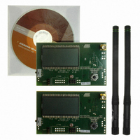
KIT DEMO 315MHZ BLACKBIRD
Manufacturer
Atmel
Type
Transceiver, UHFr
Specifications of ATAB5423-3-WB
Frequency
315MHz
Product
RF Modules
For Use With/related Products
ATA5423
Lead Free Status / RoHS Status
Lead free / RoHS Compliant
Other names
ATAB-5423-3-WB


3.7
3.8
3.9
4841D–WIRE–10/07
In-band Disturbers, Data Filter, Quasi-peak Detector, Data Slicer
DEM_OUT Output
RSSI Output
If a disturbing signal falls into the received band or a blocker is not continuous wave, the perfor-
mance of a receiver strongly depends on the circuits after the IF filter. The demodulator, data
filter and data slicer are important, in that case.
The data filter of the ATA5423/ATA5425/ATA5428/ATA5429 implies a quasi-peak detector. This
results in a good suppression of the above mentioned disturbers and exhibits a good carrier to
Gaussian noise performance. The required useful signal to disturbing signal ratio to be received
with a BER of 10
BR_Range_2)/6 dB (BR_Range_3) in FSK mode. Due to the many different waveforms possible
these numbers are measured for signal as well as for disturbers with peak amplitude values.
Note that these values are worst case values and are valid for any type of modulation and mod-
ulating frequency of the disturbing signal as well as the receiving signal. For many combinations,
lower carrier to disturbing signal ratios are needed.
The internal raw output signal of the demodulator Demod_Out is available at pin DEM_OUT.
DEM_OUT is an open drain output and must be connected to a pull-up resistor if it is used (typi-
cally 100 k ) otherwise no signal is present at that pin.
The output voltage of the pin RSSI is an analog voltage, proportional to the input power level.
Using the RSSI output signal, the signal strength of different transmitters can be distinguished.
The usable dynamic range of the RSSI amplifier is 70 dB, the input power range P(RF
–115 dBm to –45 dBm and the gain is 8 mV/dB.
typical device at 433.92 MHz with VS1 = VS2 = 2.4 to 3.6 V and T
matched input according to
3.3 dB and at 868.3 MHz about 2.7 dB more signal level, at 345 MHz about 0.8 dB and at
315 MHz about 1 dB less signal level is needed for the same RSSI results.
Figure 3-6.
Typical RSSI Characteristic versus Temperature and Supply Voltage
–3
is less than 12 dB in ASK mode and less than 3 dB (BR_Range_0 to
1100
1000
ATA5423/ATA5425/ATA5428/ATA5429
900
800
700
600
500
400
-120
Table 3-2 on page 12
-110
min.
-100
-90
P
typ.
RF_IN
Figure 3-6
and
-80
(dBm)
Figure 3-1 on page
-70
max.
shows the RSSI characteristic of a
-60
amb
-50
= –40°C to +85°C with a
11. At 915 MHz about
-40
IN
) is
17
Related parts for ATAB5423-3-WB
Image
Part Number
Description
Manufacturer
Datasheet
Request
R

Part Number:
Description:
BOARD BASESTATN UHF RCVR 315MHZ
Manufacturer:
Atmel
Datasheet:

Part Number:
Description:
DEV KIT FOR AVR/AVR32
Manufacturer:
Atmel
Datasheet:

Part Number:
Description:
INTERVAL AND WIPE/WASH WIPER CONTROL IC WITH DELAY
Manufacturer:
ATMEL Corporation
Datasheet:
Part Number:
Description:
Low-Voltage Voice-Switched IC for Hands-Free Operation
Manufacturer:
ATMEL Corporation
Datasheet:
Part Number:
Description:
MONOLITHIC INTEGRATED FEATUREPHONE CIRCUIT
Manufacturer:
ATMEL Corporation
Datasheet:
Part Number:
Description:
AM-FM Receiver IC U4255BM-M
Manufacturer:
ATMEL Corporation
Datasheet:
Part Number:
Description:
Monolithic Integrated Feature Phone Circuit
Manufacturer:
ATMEL Corporation
Datasheet:
Part Number:
Description:
Multistandard Video-IF and Quasi Parallel Sound Processing
Manufacturer:
ATMEL Corporation
Datasheet:
Part Number:
Description:
High-performance EE PLD
Manufacturer:
ATMEL Corporation
Datasheet:
Part Number:
Description:
8-bit Flash Microcontroller
Manufacturer:
ATMEL Corporation
Datasheet:
Part Number:
Description:
2-Wire Serial EEPROM
Manufacturer:
ATMEL Corporation
Datasheet: