ATAB5423-3-WB Atmel, ATAB5423-3-WB Datasheet - Page 29
ATAB5423-3-WB
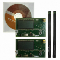
Manufacturer Part Number
ATAB5423-3-WB
Description
KIT DEMO 315MHZ BLACKBIRD
Manufacturer
Atmel
Type
Transceiver, UHFr
Specifications of ATAB5423-3-WB
Frequency
315MHz
Product
RF Modules
For Use With/related Products
ATA5423
Lead Free Status / RoHS Status
Lead free / RoHS Compliant
Other names
ATAB-5423-3-WB


4.1
Figure 4-3.
4.2
4841D–WIRE–10/07
Pin CLK
Basic Clock Cycle of the Digital Circuitry
(Control register 3)
Clock Timing
N_RESET
CLK_ON
VSOUT
CLK
Pin CLK is an output to clock a connected microcontroller. The clock frequency f
as follows:
Because the enabling of pin CLK is asynchronous, the first clock cycle may be incomplete. The
signal at CLK output has a nominal 50% duty cycle.
The complete timing of the digital circuitry is derived from one clock. As shown in
on page
a divider.
T
The clock cycle of the bit check and the TX bit rate depends on the selected bit-rate range
(BR_Range) which is defined in control register 6 (see
is defined in control register 4 (see
the following formulas for further reference:
BR_Range
f
f
DCLK
DCLK
CLK
• Timing of the polling circuit including bit check
• TX bit rate
V
Thres_2
=
=
controls the following application relevant parameters:
f
---------- -
f
---------- -
XTO
27, this clock cycle T
= 2.38V (typically)
XTO
16
3
V
Thres_1
ATA5423/ATA5425/ATA5428/ATA5429
= 2.3V (typically)
DCLK
is derived from the crystal oscillator (XTO) in combination with
Table 7-13 on page
BR_Range 0: T
BR_Range 1: T
BR_Range 2: T
BR_Range 3: T
XDCLK
XDCLK
XDCLK
XDCLK
40). This clock cycle T
Table 7-20 on page
= 8
= 4
= 2
= 1
T
T
T
T
DCLK
DCLK
DCLK
DCLK
X
X
X
X
42) and XLim which
Lim
Lim
Lim
Lim
XDCLK
CLK
is defined by
is calculated
Figure 4-2
29
Related parts for ATAB5423-3-WB
Image
Part Number
Description
Manufacturer
Datasheet
Request
R

Part Number:
Description:
BOARD BASESTATN UHF RCVR 315MHZ
Manufacturer:
Atmel
Datasheet:

Part Number:
Description:
DEV KIT FOR AVR/AVR32
Manufacturer:
Atmel
Datasheet:

Part Number:
Description:
INTERVAL AND WIPE/WASH WIPER CONTROL IC WITH DELAY
Manufacturer:
ATMEL Corporation
Datasheet:
Part Number:
Description:
Low-Voltage Voice-Switched IC for Hands-Free Operation
Manufacturer:
ATMEL Corporation
Datasheet:
Part Number:
Description:
MONOLITHIC INTEGRATED FEATUREPHONE CIRCUIT
Manufacturer:
ATMEL Corporation
Datasheet:
Part Number:
Description:
AM-FM Receiver IC U4255BM-M
Manufacturer:
ATMEL Corporation
Datasheet:
Part Number:
Description:
Monolithic Integrated Feature Phone Circuit
Manufacturer:
ATMEL Corporation
Datasheet:
Part Number:
Description:
Multistandard Video-IF and Quasi Parallel Sound Processing
Manufacturer:
ATMEL Corporation
Datasheet:
Part Number:
Description:
High-performance EE PLD
Manufacturer:
ATMEL Corporation
Datasheet:
Part Number:
Description:
8-bit Flash Microcontroller
Manufacturer:
ATMEL Corporation
Datasheet:
Part Number:
Description:
2-Wire Serial EEPROM
Manufacturer:
ATMEL Corporation
Datasheet: