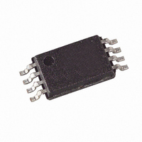
T48C862M-R3-TNS Atmel, T48C862M-R3-TNS Datasheet - Page 67

T48C862M-R3-TNS
Manufacturer Part Number
T48C862M-R3-TNS
Description
IC MON TIRE PRESS 315MHZ 24SOIC
Manufacturer
Atmel
Datasheet
1.T48C862M-R3-TNS.pdf
(107 pages)
Specifications of T48C862M-R3-TNS
Frequency
315MHz
Modulation Or Protocol
FM, FSK
Data Rate - Maximum
32 kBaud
Power - Output
10dBm
Current - Transmitting
9.5mA
Data Interface
PCB, Surface Mount
Antenna Connector
PCB, Surface Mount
Memory Size
1KB EEPROM, 1KB RAM
Voltage - Supply
2 V ~ 4 V
Operating Temperature
-40°C ~ 125°C
Package / Case
24-SOIC (0.200", 5.30mm Width)
Lead Free Status / RoHS Status
Contains lead / RoHS non-compliant
Features
-
Applications
-
SSI Peripheral Configuration
4554A–4BMCU–02/03
The synchronous serial interface (SSI) can be used either for serial communication with
external devices such as EEPROMs, shift registers, display drivers, other microcontrol-
lers, or as a means for generating and capturing on-chip serial streams of data. External
data communication takes place via the Port 4 (BP4),a multi-functional port which can
be software configured by writing the appropriate control word into the P4CR register.
The SSI can be configured in any of the following ways:
1. 2-wire external interface for bi-directional data communication with one data ter-
2. 3-wire external interface for simultaneous input and output of serial data, with a
3. Timer/SSI combined modes – the SSI used together with Timer 2 or Timer 3 is
4. Multi-chip link (MCL) – the SSI can also be used as an interchip data interface for
Figure 64. Block Diagram of the Synchronous Serial Interface
T1OUT
SYSCL
POUT
TOG2
minal and one shift clock. The SSI uses the Port BP43 as a bi-directional serial
data line (SD) and BP40 as shift clock line (SC).
serial input data terminal (SI), a serial output data terminal (SO) and a shift clock
(SC). The SSI uses BP40 as shift clock (SC), while the serial data input (SI) is
applied to BP43 (configured in P4CR as input!). Serial output data (SO) in this
case is passed through to BP42 (configured in P4CR to T2O) via the Timer 2
output stage (T2M2 configured in mode 6).
capable of performing a variety of data modulation and demodulation functions
(see Timer Section). The modulating data is converted by the SSI into a continu-
ous serial stream of data which is in turn modulated in one of the timer functional
blocks. Serial demodulated data can be serially captured in the SSI and read by
the controller. In the Timer 3 modes 10 and 11 (demodulation modes) the SSI
can only be used as demodulator.
use in single package multi-chip modules or hybrids. For such applications, the
SSI is provided with two dedicated pads (MCL_SD and MCL_SC) which act as a
two-wire chip-to-chip link. The MCL can be activated by the MCL control bit.
Should these MCL pads be used by the SSI, the standard SD and SC pins are
not required and the corresponding Port 4 ports are available as conventional
data ports.
SIC1
/2
SC
Shift_CL
SO
Transmit
Buffer
I/O-bus
SIC2
MSB
STB
SSI-Control
8-bit Shift Register
I/O-bus
SISC
SRB
Control
LSB
Receive
Buffer
Timer 2 / Timer 3
SI
INT3
T48C862-R3
SO
Output
SI
SCI
SC
MCL_SC
MCL_SD
SD
67


