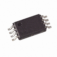
T48C862M-R3-TNS Atmel, T48C862M-R3-TNS Datasheet - Page 95

T48C862M-R3-TNS
Manufacturer Part Number
T48C862M-R3-TNS
Description
IC MON TIRE PRESS 315MHZ 24SOIC
Manufacturer
Atmel
Datasheet
1.T48C862M-R3-TNS.pdf
(107 pages)
Specifications of T48C862M-R3-TNS
Frequency
315MHz
Modulation Or Protocol
FM, FSK
Data Rate - Maximum
32 kBaud
Power - Output
10dBm
Current - Transmitting
9.5mA
Data Interface
PCB, Surface Mount
Antenna Connector
PCB, Surface Mount
Memory Size
1KB EEPROM, 1KB RAM
Voltage - Supply
2 V ~ 4 V
Operating Temperature
-40°C ~ 125°C
Package / Case
24-SOIC (0.200", 5.30mm Width)
Lead Free Status / RoHS Status
Contains lead / RoHS non-compliant
Features
-
Applications
-
- Current page: 95 of 107
- Download datasheet (2Mb)
Absolute Maximum Ratings
Voltages are given relative to V
Note:
Thermal Resistance
DC Operating Characteristics
V
4554A–4BMCU–02/03
Parameters
Supply voltage
Input voltage (on any pin)
Output short circuit duration
Operating temperature range
Storage temperature range
Soldering temperature (t £ 10 s)
Parameter
Thermal resistance (SSO20)
Parameters
Power Supply
Operating voltage at V
Active current
CPU active
Power down current
(CPU sleep,
RC oscillator active,
4-MHz quartz oscillator active)
Sleep current
(CPU sleep,
32-kHz quartz oscillator active
4-MHz quartz oscillator inactive)
Sleep current
(CPU sleep,
32-kHz quartz oscillator inactive
4-MHz quartz oscillator inactive)
Pin capacitance
SS
= 0 V, T
Stresses greater than those listed under absolute maximum ratings may cause permanent damage to the device. This is a
stress rating only and functional operation of the device at any condition above those indicated in the operational section of this
specification is not implied. Exposure to absolute maximum rating condition for an extended period may affect device reliability.
All inputs and outputs are protected against high electrostatic voltages or electric fields. However, precautions to minimize the
build-up of electrostatic charges during handling are recommended. Reliability of operation is enhanced if unused inputs are
connected to an appropriate logic voltage level (e.g., V
amb
= -40 ° C to +125 ° C unless otherwise specified.
DD
SS
Test Conditions
f
V
V
f
V
V
V
V
V
V
V
Any pin to V
SYSCL
SYSCL
DD
DD
DD
DD
DD
DD
DD
DD
DD
= 3.0 V
= 1.8 V
= 1.8 V
= 3.0 V
= 1.8 V
= 3.0 V
= 3.0 V at 85 ° C
= 3.0 V
= 3.0 V at 85 ° C
= 1 MHz
= 1 MHz
SS
Symbol
Symbol
R
T
t
V
T
T
V
short
amb
thJA
DD
stg
sld
IN
DD
).
V
SS
Symbol
I
I
V
Sleep
Sleep
I
I
-0.3 £ V
C
DD
PD
DD
L
-0.3 to + 6.5
-40 to +125
-40 to +150
Indefinite
Value
Value
260
140
IN
£ V
V
Min.
2.0
POR
DD
+0.3
Typ.
0.3
0.4
0.4
0.6
0.3
40
70
7
T48C862-R3
Max.
150
0.4
4.0
4.3
1.5
3.5
1.0
10
Unit
Unit
K/W
° C
° C
° C
V
V
s
Unit
mA
mA
µA
µA
µA
µA
µA
µA
µA
pF
V
V
95
Related parts for T48C862M-R3-TNS
Image
Part Number
Description
Manufacturer
Datasheet
Request
R

Part Number:
Description:
IC MON TIRE PRESS 433MHZ 24-SOIC
Manufacturer:
Atmel
Datasheet:

Part Number:
Description:
IC MON TIRE PRESS 433MHZ 24-SOIC
Manufacturer:
Atmel
Datasheet:

Part Number:
Description:
IC MON TIRE PRESS 315MHZ 24SOIC
Manufacturer:
Atmel
Datasheet:

Part Number:
Description:
DEV KIT FOR AVR/AVR32
Manufacturer:
Atmel
Datasheet:

Part Number:
Description:
INTERVAL AND WIPE/WASH WIPER CONTROL IC WITH DELAY
Manufacturer:
ATMEL Corporation
Datasheet:

Part Number:
Description:
Low-Voltage Voice-Switched IC for Hands-Free Operation
Manufacturer:
ATMEL Corporation
Datasheet:

Part Number:
Description:
MONOLITHIC INTEGRATED FEATUREPHONE CIRCUIT
Manufacturer:
ATMEL Corporation
Datasheet:

Part Number:
Description:
AM-FM Receiver IC U4255BM-M
Manufacturer:
ATMEL Corporation
Datasheet:

Part Number:
Description:
Monolithic Integrated Feature Phone Circuit
Manufacturer:
ATMEL Corporation
Datasheet:

Part Number:
Description:
Multistandard Video-IF and Quasi Parallel Sound Processing
Manufacturer:
ATMEL Corporation
Datasheet:

Part Number:
Description:
High-performance EE PLD
Manufacturer:
ATMEL Corporation
Datasheet:

Part Number:
Description:
8-bit Flash Microcontroller
Manufacturer:
ATMEL Corporation
Datasheet:


