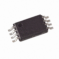
T48C862M-R3-TNS Atmel, T48C862M-R3-TNS Datasheet - Page 82

T48C862M-R3-TNS
Manufacturer Part Number
T48C862M-R3-TNS
Description
IC MON TIRE PRESS 315MHZ 24SOIC
Manufacturer
Atmel
Datasheet
1.T48C862M-R3-TNS.pdf
(107 pages)
Specifications of T48C862M-R3-TNS
Frequency
315MHz
Modulation Or Protocol
FM, FSK
Data Rate - Maximum
32 kBaud
Power - Output
10dBm
Current - Transmitting
9.5mA
Data Interface
PCB, Surface Mount
Antenna Connector
PCB, Surface Mount
Memory Size
1KB EEPROM, 1KB RAM
Voltage - Supply
2 V ~ 4 V
Operating Temperature
-40°C ~ 125°C
Package / Case
24-SOIC (0.200", 5.30mm Width)
Lead Free Status / RoHS Status
Contains lead / RoHS non-compliant
Features
-
Applications
-
- Current page: 82 of 107
- Download datasheet (2Mb)
Combination Mode Timer 3 and SSI
Figure 79. Combination Timer 3 and SSI
Combination Mode 6:
FSK Modulation
82
T3I
T48C862-R3
T1OUT
SYSCL
POUT
T3EX
T3CS
CL3
RES
Compare 3/1
T3CO1
T1OUT
SYSCL
TOG2
POUT
8-bit counter 3
SSI mode 1:
Timer 3 mode 8: FSK modulation with shift register data (SO)
The two compare registers are used to generate two varied time intervals. The SSI data
output selects which compare register is used for the output frequency generation. A "0"
level at the SSI data output enables the compare register 1 and a "1" level enables the
compare register 2. The compare and compare mode registers must be programmed to
generate the two frequencies via the output toggle flip-lop. The SSI can be supplied with
the toggle signal of Timer 2 or any other clock source. The Timer 3 counter is driven by
an internal or external clock source.
T3CP
Compare 3/2
SCLI
T3CO2
SIC1
CP3
I/O-bus
Shift_CL
Transmit buffer
8-bit shift register internal data output (SO) to the Timer 3
SO
SIC2
MSB
T3CM1
T3C
Timer 3 - control
STB
SSI-control
8-bit shift register
I/O-bus
T3CM2
SISC
T3ST
SRB
LSB
Receive buffer
Control
SI
INT3
T3M
Output
T3EX
T3I
CM31
RES
INT5
TOG3
Control
M2
SO
SI
SC
Modulator 3
Demodu-
lator 3
MCL_SC
MCL_SD
SC
SI
4554A–4BMCU–02/03
T3O
SC
SI
Related parts for T48C862M-R3-TNS
Image
Part Number
Description
Manufacturer
Datasheet
Request
R

Part Number:
Description:
IC MON TIRE PRESS 433MHZ 24-SOIC
Manufacturer:
Atmel
Datasheet:

Part Number:
Description:
IC MON TIRE PRESS 433MHZ 24-SOIC
Manufacturer:
Atmel
Datasheet:

Part Number:
Description:
IC MON TIRE PRESS 315MHZ 24SOIC
Manufacturer:
Atmel
Datasheet:

Part Number:
Description:
DEV KIT FOR AVR/AVR32
Manufacturer:
Atmel
Datasheet:

Part Number:
Description:
INTERVAL AND WIPE/WASH WIPER CONTROL IC WITH DELAY
Manufacturer:
ATMEL Corporation
Datasheet:

Part Number:
Description:
Low-Voltage Voice-Switched IC for Hands-Free Operation
Manufacturer:
ATMEL Corporation
Datasheet:

Part Number:
Description:
MONOLITHIC INTEGRATED FEATUREPHONE CIRCUIT
Manufacturer:
ATMEL Corporation
Datasheet:

Part Number:
Description:
AM-FM Receiver IC U4255BM-M
Manufacturer:
ATMEL Corporation
Datasheet:

Part Number:
Description:
Monolithic Integrated Feature Phone Circuit
Manufacturer:
ATMEL Corporation
Datasheet:

Part Number:
Description:
Multistandard Video-IF and Quasi Parallel Sound Processing
Manufacturer:
ATMEL Corporation
Datasheet:

Part Number:
Description:
High-performance EE PLD
Manufacturer:
ATMEL Corporation
Datasheet:

Part Number:
Description:
8-bit Flash Microcontroller
Manufacturer:
ATMEL Corporation
Datasheet:


