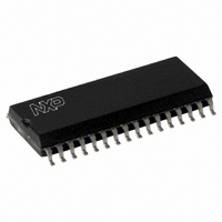
MFRC50001T/0FE,112 NXP Semiconductors, MFRC50001T/0FE,112 Datasheet - Page 97

MFRC50001T/0FE,112
Manufacturer Part Number
MFRC50001T/0FE,112
Description
IC MIFARE READER 32-SOIC
Manufacturer
NXP Semiconductors
Series
MIFARE®r
Specifications of MFRC50001T/0FE,112
Rf Type
Read Only
Frequency
13.56MHz
Features
ISO14443-A, ISO14443-B, ISO15693
Package / Case
32-SOIC (0.300", 7.50mm Width)
Product
RFID Readers
Operating Temperature Range
- 25 C to + 85 C
Lead Free Status / RoHS Status
Lead free / RoHS Compliant
Lead Free Status / RoHS Status
Lead free / RoHS Compliant, Lead free / RoHS Compliant
Other names
568-2222-5
935268039112
MFRC500
MFRC51T0FED
935268039112
MFRC500
MFRC51T0FED
Available stocks
Company
Part Number
Manufacturer
Quantity
Price
Part Number:
MFRC50001T/0FE,112
Manufacturer:
NXP/恩智浦
Quantity:
20 000
NXP Semiconductors
MFRC500_33
Product data sheet
PUBLIC
15.2.3 Digital test signals
15.2.4 Analog and digital test signal Examples
Table 161. Analog test signal selection
Digital test signals can be routed to pin MFOUT by setting bit SignalToMFOUT = logic 1. A
digital test signal is selected using the TestDigiSelect register TestDigiSignalSel[6:0] bits.
The signals selected by the TestDigiSignalSel[6:0] bits are shown in
Table 162. Digital test signal selection
If test signals are not used, the TestDigiSelect register address value must be 00h.
Remark: All other values for TestDigiSignalSel[6:0] are for production test purposes only.
Figure 25
receiving path. RX reference is given to show the Manchester modulated signal on pin
RX.
The signal is demodulated and amplified in the receiver circuitry. Signal VRXAmpQ is the
amplified side-band signal using the Q-clock for demodulation. The signals VCorrDQ and
VCorrNQ were generated in the correlation circuitry. They are processed further in the
evaluation and digitizer circuitry.
Signals VEvalR and VEvalL show the evaluation of the signal’s right and left half-bit.
Finally, the digital test signal s_data shows the received data. This is then sent to the
internal digital circuit and s_valid which indicates the received data stream is valid.
Value
B
C
D
E
F
TestDigiSignalSel
[6:0]
F4h
E4h
D4h
C4h
B5h
A5h
96h
00h
Signal Name
VEvalR
VTemp
reserved
reserved
reserved
shows a MIFARE card’s answer to a request command using the Q-clock
All information provided in this document is subject to legal disclaimers.
Signal name
s_data
s_valid
s_coll
s_clock
rd_sync
wr_sync
int_clock
no test signal
Rev. 3.3 — 15 March 2010
Description
evaluation signal from the right half-bit
temperature voltage derived from band gap
reserved for future use
reserved for future use
reserved for future use
048033
Description
data received from the card
when logic 1 is returned the s_data and s_coll signals are
valid
when logic 1 is returned a collision has been detected in the
current bit
internal serial clock:
internal synchronized read signal which is derived from the
parallel microprocessor interface
internal synchronized write signal which is derived from the
parallel microprocessor interface
internal 13.56 MHz clock
output as defined by the MFOUTSelect register
MFOUTSelect[2:0] bits routed to pin MFOUT
during transmission, this is the encoder clock
during reception this is the receiver clock
…continued
Highly Integrated ISO/IEC 14443 A Reader IC
Table
MFRC500
© NXP B.V. 2010. All rights reserved.
162.
97 of 110


