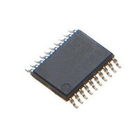
MCP4441T-503E/ST Microchip Technology, MCP4441T-503E/ST Datasheet - Page 39

MCP4441T-503E/ST
Manufacturer Part Number
MCP4441T-503E/ST
Description
IC DGTL POT 129TAPS QUAD 20TSSOP
Manufacturer
Microchip Technology
Datasheet
1.MCP4441-103EML.pdf
(100 pages)
Specifications of MCP4441T-503E/ST
Package / Case
20-TSSOP (0.173", 4.40mm Width)
Temperature Coefficient
150 ppm/°C Typical
Taps
129
Resistance (ohms)
50K
Number Of Circuits
4
Memory Type
Non-Volatile
Interface
I²C, 2-Wire Serial
Voltage - Supply
2.7 V ~ 5.5 V
Operating Temperature
-40°C ~ 125°C
Mounting Type
Surface Mount
Number Of Pots
Quad
Taps Per Pot
129
Resistance
50 KOhms
Wiper Memory
Non Volatile
Buffered Wiper
Buffered
Digital Interface
I2C
Operating Supply Voltage
2.7 V to 5.5 V
Supply Current
600 uA
Maximum Operating Temperature
+ 125 C
Minimum Operating Temperature
- 40 C
Description/function
Quad I2C Digital POT with Nonvolatile Memory
Mounting Style
SMD/SMT
Supply Voltage (max)
5.5 V
Supply Voltage (min)
2.7 V
Lead Free Status / RoHS Status
Lead free / RoHS Compliant
Available stocks
Company
Part Number
Manufacturer
Quantity
Price
Part Number:
MCP4441T-503E/ST
Manufacturer:
MICROCHIP/微芯
Quantity:
20 000
3.0
The descriptions of the pins are listed in
Additional descriptions of the device pins follows.
TABLE 3-1:
© 2010 Microchip Technology Inc.
Legend:
Note 1:
14L
—
—
—
10
—
—
11
12
13
14
—
—
1
2
3
4
5
6
7
8
9
TSSOP
2:
PIN DESCRIPTIONS
20L
10
11
12
13
14
15
16
17
18
19
20
—
1
2
3
4
5
6
7
8
9
The pin’s “smart” pull-up shuts off while the pin is forced low. This is done to reduce the standby and
shut-down current.
The QFN package has a contact on the bottom of the package. This contact is conductively connected to
the die substrate, and therefore should be unconnected or connected to the same ground as the device’s
V
SS
HV w/ST = High Voltage tolerant input (with Schmidtt trigger input)
A = Analog pins (Potentiometer terminals)
O = digital output
P = Power
pin.
QFN
20L
PINOUT DESCRIPTION FOR THE MCP444X/446X
19
20
10
12
13
14
15
16
17
18
21
11
1
2
3
4
5
6
7
8
9
Pin
Symbol
HVC/A0
RESET
P3W
P1W
P0W
P2W
SDA
P3A
P3B
SCL
P1B
P1A
P0A
P0B
P2B
P2A
V
V
WP
A1
EP
DD
SS
I/O
—
—
—
A
A
A
A
A
A
A
A
A
A
A
A
I
I
I
I
I
I
Table
HV w/ST
HV w/ST
HV w/ST
HV w/ST
HV w/ST
HV w/ST
Analog
Analog
Analog
Analog
Analog
Analog
Analog
Analog
Analog
Analog
Analog
Analog
Buffer
Type
3-1.
—
P
P
Pull-up/
(Note
“smart” High Voltage Command / I
“smart” Hardware EEPROM Write Protect
“smart” I
Weak
down
Yes
No
No
No
No
No
No
No
No
No
No
No
No
No
No
—
—
—
1)
I = digital input (high Z)
I/O = Input / Output
Potentiometer 3 Terminal A
Potentiometer 3 Wiper Terminal
Potentiometer 3 Terminal B
I
I
Ground
Potentiometer 1 Terminal B
Potentiometer 1 Wiper Terminal
Potentiometer 1 Terminal A
Potentiometer 0 Terminal A
Potentiometer 0 Wiper Terminal
Potentiometer 0 Terminal B
Hardware Reset Pin
Positive Power Supply Input
Potentiometer 2 Terminal B
Potentiometer 2 Wiper Terminal
Potentiometer 2 Terminal A
Exposed Pad.
2
2
2
C Clock Input
C Serial Data I/O. Open Drain output
C Address 1
MCP444X/446X
Standard Function
(Note
2)
2
C Address 0
DS22265A-page 39


