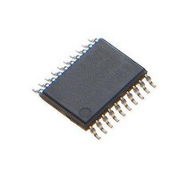
MCP4441T-503E/ST Microchip Technology, MCP4441T-503E/ST Datasheet - Page 40

MCP4441T-503E/ST
Manufacturer Part Number
MCP4441T-503E/ST
Description
IC DGTL POT 129TAPS QUAD 20TSSOP
Manufacturer
Microchip Technology
Datasheet
1.MCP4441-103EML.pdf
(100 pages)
Specifications of MCP4441T-503E/ST
Package / Case
20-TSSOP (0.173", 4.40mm Width)
Temperature Coefficient
150 ppm/°C Typical
Taps
129
Resistance (ohms)
50K
Number Of Circuits
4
Memory Type
Non-Volatile
Interface
I²C, 2-Wire Serial
Voltage - Supply
2.7 V ~ 5.5 V
Operating Temperature
-40°C ~ 125°C
Mounting Type
Surface Mount
Number Of Pots
Quad
Taps Per Pot
129
Resistance
50 KOhms
Wiper Memory
Non Volatile
Buffered Wiper
Buffered
Digital Interface
I2C
Operating Supply Voltage
2.7 V to 5.5 V
Supply Current
600 uA
Maximum Operating Temperature
+ 125 C
Minimum Operating Temperature
- 40 C
Description/function
Quad I2C Digital POT with Nonvolatile Memory
Mounting Style
SMD/SMT
Supply Voltage (max)
5.5 V
Supply Voltage (min)
2.7 V
Lead Free Status / RoHS Status
Lead free / RoHS Compliant
Available stocks
Company
Part Number
Manufacturer
Quantity
Price
Part Number:
MCP4441T-503E/ST
Manufacturer:
MICROCHIP/微芯
Quantity:
20 000
MCP444X/446X
3.1
The HVC/A0 pin is the Address 0 input for the I
interface as well as the High Voltage Command pin. At
the device’s POR/BOR the value of the A0 address bit
is latched. This input along with the A1 pin completes
the device address. This allows up to 4 MCP44XX
devices to be on a single I
During normal operation, the voltage on this pin
determines whether the I
command or a High Voltage command (when HVC/A0
= V
3.2
The SCL pin is the serial interfaces Serial Clock pin.
This pin is connected to the Host Controllers SCL pin.
The MCP44XX is a slave device, so its SCL pin accepts
only external clock signals.
3.3
The SDA pin is the serial interfaces Serial Data pin.
This pin is connected to the Host Controllers SDA pin.
The SDA pin is an open-drain N-channel driver.
3.4
The V
3.5
The terminal B pin is connected to the internal
potentiometer’s terminal B.
The potentiometer’s terminal B is the fixed connection
to the Zero Scale wiper value of the digital
potentiometer. This corresponds to a wiper value of
0x00 for both 7-bit and 8-bit devices.
The terminal B pin does not have a polarity relative to
the terminal W or A pins. The terminal B pin can
support both positive and negative current. The voltage
on terminal B must be between V
MCP44XX devices have four terminal B pins, one for
each resistor network.
3.6
The terminal W pin is connected to the internal
potentiometer’s terminal W (the wiper). The wiper
terminal is the adjustable terminal of the digital
potentiometer. The terminal W pin does not have a
polarity relative to terminals A or B pins. The terminal
W pin can support both positive and negative current.
The voltage on terminal W must be between V
V
MCP44XX devices have four terminal W pins, one for
each resistor network.
DS22265A-page 40
DD
IHH
.
SS
).
High Voltage Command /
Address 0 (HVC/A0)
Serial Clock (SCL)
Serial Data (SDA)
Ground (V
pin is the device ground reference.
Potentiometer Terminal B
Potentiometer Wiper (W) Terminal
SS
)
2
2
C bus.
C command is a normal
SS
and V
DD
.
SS
and
2
C
3.7
The terminal A pin is available on the MCP44X1
devices,
potentiometer’s terminal A.
The potentiometer’s terminal A is the fixed connection
to the Full Scale wiper value of the digital
potentiometer. This corresponds to a wiper value of
0x100 for 8-bit devices or 0x80 for 7-bit devices.
The terminal A pin does not have a polarity relative to
the terminal W or B pins. The terminal A pin can
support both positive and negative current. The voltage
on terminal A must be between V
The terminal A pin is not available on the MCP44X2
devices, and the internally terminal A signal is floating.
MCP44X1 devices have four terminal A pins, one for
each resistor network. Terminal A is not available on
the MCP44X2 devices.
3.8
The WP pin is used to force the nonvolatile memory to
be write protected.
3.9
The RESET pin is used to force the device into the
POR/BOR state.
3.10
The A1 pin is the I
with the A0 pins, up to 4 MCP44XX devices can be on
a single I
3.11
The V
The input power supply is relative to V
While the device V
performance of the device may not meet the data sheet
specifications.
3.12
These pins should be either connected to V
3.13
This pad is conductively connected to the device's
substrate. This pad should be tied to the same potential
as the V
used to assist as a heat sink for the device when
connected to a PCB heat sink.
DD
SS
Potentiometer Terminal A
Write Protect (WP)
Address 1 (A1)
2
Positive Power Supply Input (V
pin is the device’s positive power supply input.
No Connect (NC)
Exposed Pad (EP)
Reset (RESET)
C bus.
pin (or left unconnected). This pad could be
and
is
2
C interface’s Address 1 pin. Along
DD
connected
© 2010 Microchip Technology Inc.
< V
min
(2.7V), the electrical
SS
to
and V
SS
.
the
DD
DD
.
or V
internal
DD
SS
)
.


