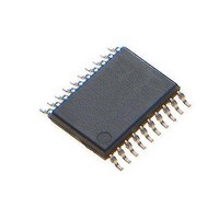
MCP4441T-503E/ST Microchip Technology, MCP4441T-503E/ST Datasheet - Page 78

MCP4441T-503E/ST
Manufacturer Part Number
MCP4441T-503E/ST
Description
IC DGTL POT 129TAPS QUAD 20TSSOP
Manufacturer
Microchip Technology
Datasheet
1.MCP4441-103EML.pdf
(100 pages)
Specifications of MCP4441T-503E/ST
Package / Case
20-TSSOP (0.173", 4.40mm Width)
Temperature Coefficient
150 ppm/°C Typical
Taps
129
Resistance (ohms)
50K
Number Of Circuits
4
Memory Type
Non-Volatile
Interface
I²C, 2-Wire Serial
Voltage - Supply
2.7 V ~ 5.5 V
Operating Temperature
-40°C ~ 125°C
Mounting Type
Surface Mount
Number Of Pots
Quad
Taps Per Pot
129
Resistance
50 KOhms
Wiper Memory
Non Volatile
Buffered Wiper
Buffered
Digital Interface
I2C
Operating Supply Voltage
2.7 V to 5.5 V
Supply Current
600 uA
Maximum Operating Temperature
+ 125 C
Minimum Operating Temperature
- 40 C
Description/function
Quad I2C Digital POT with Nonvolatile Memory
Mounting Style
SMD/SMT
Supply Voltage (max)
5.5 V
Supply Voltage (min)
2.7 V
Lead Free Status / RoHS Status
Lead free / RoHS Compliant
Available stocks
Company
Part Number
Manufacturer
Quantity
Price
Part Number:
MCP4441T-503E/ST
Manufacturer:
MICROCHIP/微芯
Quantity:
20 000
MCP444X/446X
8.6
In the design of a system with the MCP44XX devices,
the following considerations should be taken into
account:
•
•
8.6.1
The typical application will require a bypass capacitor
in order to filter high-frequency noise, which can be
induced onto the power supply's traces. The bypass
capacitor helps to minimize the effect of these noise
sources on signal integrity.
appropriate bypass strategy.
In this example, the recommended bypass capacitor
value is 0.1 µF. This capacitor should be placed as
close (within 4 mm) to the device power pin (V
possible.
The power source supplying these devices should be
as clean as possible. If the application circuit has
separate digital and analog power supplies, V
V
FIGURE 8-8:
Connections.
DS22265A-page 78
SS
Power Supply Considerations
Layout Considerations
should reside on the analog plane.
W
A
B
Design Considerations
POWER SUPPLY
CONSIDERATIONS
0.1 µF
V
V
Typical Microcontroller
DD
SS
Figure 8-8
HVC/A0
0.1 µF
SDA
SCL
A1
illustrates an
V
V
DD
SS
DD
DD
) as
and
8.6.2
Several layout considerations may be applicable to
your application. These may include:
•
•
•
8.6.2.1
Inductively-coupled AC transients and digital switching
noise can degrade the input and output signal integrity,
potentially masking the MCP44XX’s performance.
Careful board layout minimizes these effects and
increases the Signal-to-Noise Ratio (SNR). Multi-layer
boards utilizing a low-inductance ground plane,
isolated inputs, isolated outputs and proper decoupling
are critical to achieving the performance that the silicon
is
environments may require shielding of critical signals.
If low noise is desired, breadboards and wire-wrapped
boards are not recommended.
8.6.2.2
The specification of the MCP44XX pinouts was done to
allow systems to be designed to easily support the use
of either the dual (MCP46XX) or quad (MCP44XX)
device.
Figure 8-9
quad device footprint. For the Rheostat devices, the
dual device is in the MSOP package, so the footprints
would need to be offset from each other.
FIGURE 8-9:
Package) vs. Dual Pinout.
HVC/A0
HVC/A0
Noise
Footprint Compatibility
PCB Area Requirements
P3W
Note 1: Pin 15 (RESET) is the Address A2 (A2)
SDA
SCL
P3B
P1B
P3W
P1W
V
SDA
SCL
P3A
P3B
P1B
P1A
V
capable
SS
SS
MCP44X1 Quad Potentiometers
1
2
3
4
5
6
7
MCP44X2 Quad Rheostat
1
2
3
4
5
6
7
8
9
10
shows how the dual pinout devices fit on the
TSSOP
LAYOUT CONSIDERATIONS
pin on the MCP46x1 device.
TSSOP
Noise
Footprint Compatibility
of
14
13
12
10
11
20
19
18
17
16
15
14
12
12
11
9
8
providing.
Quad Pinout (TSSOP
P2W
V
A1
P0B
P0W
P1W
P2B
P2A
P2W
V
A1
RESET
WP
P0B
P0W
P0A
P2B
© 2010 Microchip Technology Inc.
DD
DD
MCP42X2 Pinout
MCP42X1 Pinout
Particularly
harsh
(1)


