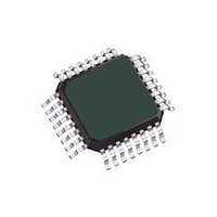
KIT33912G5DGEVME Freescale Semiconductor, KIT33912G5DGEVME Datasheet - Page 41

KIT33912G5DGEVME
Manufacturer Part Number
KIT33912G5DGEVME
Description
Power Management Modules & Development Tools 33912G5 LIN SBC KIT
Manufacturer
Freescale Semiconductor
Type
Motor / Motion Controllers & Driversr
Specifications of KIT33912G5DGEVME
Interface Type
SPI
Product
Power Management Modules
Silicon Manufacturer
Freescale
Silicon Core Number
MC33912
Kit Application Type
Interface
Application Sub Type
LIN System
Kit Contents
Board, CD, Misc Cable
Rohs Compliant
Yes
For Use With/related Products
MC33912
Lead Free Status / RoHS Status
Lead free / RoHS Compliant
MOD2, MOD1 - Mode Control Bits
clearing the watchdog in accordance with
Control Bits.
Table 12. Mode Control Bits
Voltage Status Register - VSR
register is also returned when writing to the Mode Control
Register (MCR).
VSOV - V
the VS1 pin.
VSUV - V
the VS1 pin.
VDDOT - Main Voltage Regulator Over-temperature
Warning
temperature reached the Over-temperature Prewarning
Threshold.
BATFAIL - Battery Fail Flag.
the 33912 had a Power-On-Reset (POR).
Analog Integrated Circuit Device Data
Freescale Semiconductor
MOD2
These write-only bits select the operating mode and allow
Returns the status of the several voltage monitors. This
This read-only bit indicates an over-voltage condition on
1 = Over-voltage condition.
0 = Normal condition.
This read-only bit indicates an under-voltage condition on
1 = Under-voltage condition.
0 = Normal condition.
This read-only bit indicates that the main voltage regulator
1 = Over-temperature Prewarning
0 = Normal
This read-only bit is set during power-up and indicates that
Any access to the MCR or VSR will clear the BATFAIL flag.
Table 13. Voltage Status Register - $0/$1
0
0
1
1
Read
SUP
SUP
MOD1
Under-voltage
Over-voltage
0
1
0
1
VSOV
S3
Normal Mode + Watchdog Clear
VSUV
S2
Normal Mode
Description
Sleep Mode
Stop Mode
VDDOT
S1
Table 8
BATFAIL
Mode
S0
Wake-up Control Register - WUCR
Writing the WUCR will return the Wake-Up Status Register
(WUSR).
LxWE - Wake-up Input x Enable
enabled. In Stop and Sleep mode the LxWE bit determines
which wake inputs are active for wake-up. If one of the Lx
inputs is selected on the analog multiplexer, the
corresponding LxWE is masked to 0.
Wake-up Status Register - WUSR
and is also returned when writing to the WUCR.
Lx - Wake-up input x
Lx input. If the Lx input is not enabled, then the according
Wake-up status will return 0.
allow to determine which input has caused the wake-up, by
first reading the Interrupt Status Register (ISR) and then
reading the WUSR. The source of the wake-up is only
reported on the first WUCR or WUSR access.
1 = POR Reset has occurred
0 = POR Reset has not occurred
This register is used to control the digital wake-up inputs.
This write-only bit enables/disables which Lx inputs are
1 = Wake-up Input x enabled.
0 = Wake-up Input x disabled.
This register is used to monitor the digital wake-up inputs
This read-only bit indicates the status of the corresponding
After a wake-up from Stop or Sleep mode these bits also
1 = Lx pin high, or Lx is the source of the wake-up.
0 = Lx pin low, disabled or selected as an analog input.
Table 15. Wake-up Status Register - $2/$3
Condition
Read
Reset
Value
Reset
Write
Table 14. Wake-Up Control Register - $2
L4WE
S3
C3
L4
1
POR, Reset mode or ext_reset
LOGIC COMMANDS AND REGISTERS
FUNCTIONAL DEVICE OPERATIONS
L3WE
C2
S2
L3
1
L2WE
C1
S1
1
L2
L1WE
C0
1
S0
L1
33912
41


