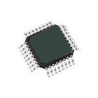
KIT33912G5DGEVME Freescale Semiconductor, KIT33912G5DGEVME Datasheet - Page 51

KIT33912G5DGEVME
Manufacturer Part Number
KIT33912G5DGEVME
Description
Power Management Modules & Development Tools 33912G5 LIN SBC KIT
Manufacturer
Freescale Semiconductor
Type
Motor / Motion Controllers & Driversr
Specifications of KIT33912G5DGEVME
Interface Type
SPI
Product
Power Management Modules
Silicon Manufacturer
Freescale
Silicon Core Number
MC33912
Kit Application Type
Interface
Application Sub Type
LIN System
Kit Contents
Board, CD, Misc Cable
Rohs Compliant
Yes
For Use With/related Products
MC33912
Lead Free Status / RoHS Status
Lead free / RoHS Compliant
Table 33. 33912 Pin Definitions
Analog Integrated Circuit Device Data
Freescale Semiconductor
Notes
73.
74.
75.
76.
77.
A functional description of each pin can be found in the
Pin
12
13
14
15
16
17
19
18
20
21
22
23
24
25
26
27
29
30
31
32
When used as digital input, a series 33 kΩ resistor must be used to protect against automotive transients.
Reverse battery protection series diodes must be used externally to protect the internal circuitry.
This pin can be connected directly to the battery line for voltage measurements. The pin is self protected against reverse battery
connections. It is strongly recommended to connect a 10kΩ resistor in series with this pin for protection purposes.
External capacitor (1.0 µF < C < 10 µF; 0.1 Ω < ESR < 5.0 Ω) required.
External capacitor (2.0 µF < C < 100 µF; 0.1 Ω < ESR < 10.0 Ω) required.
Pin Name
WDCONF
ISENSEH
ISENSEL
VSENSE
PGND
AGND
LGND
HVDD
VDD
HS2
HS1
LS2
LS1
VS2
VS1
LIN
L4
L3
L2
L1
Current Sense Pins
Hall Sensor Supply
Analog Ground Pin
Power Ground Pin
Voltage Sense Pin
High Side Outputs
Voltage Regulator
Low Side Outputs
Power Supply Pin
Configuration Pin
LIN Ground Pin
Wake-up Inputs
Formal Name
Watchdog
LIN Bus
Output
Output
This input pin is for configuration of the watchdog period and allows the
disabling of the watchdog.
This pin represents the single-wire bus transmitter and receiver.
This pin is the device LIN ground connection. It is internally connected to the
PGND pin.
Current Sense differential inputs.
Relay drivers low side outputs.
This pin is the device low side ground connection. It is internally connected to
the LGND pin.
These pins are the wake-up capable digital inputs
can be sensed analog via the analog multiplexer.
High side switch outputs.
These pins are device battery level power supply pins.VS2 is supplying the
HSx drivers while VS1 supplies the remaining blocks.
Battery voltage sense input.
+5.0 V switchable supply output pin.
+5.0 V main voltage regulator output pin.
This pin is the device analog ground connection.
Functional Pin Description on page
(75)
Definition
(76)
68.
(77)
(73)
. In addition, all Lx inputs
(74)
PIN CONNECTIONS
33912
51


