PEMB9,115 NXP Semiconductors, PEMB9,115 Datasheet - Page 3
PEMB9,115
Manufacturer Part Number
PEMB9,115
Description
Digital Transistors / Resistor Biased TRNS DOUBL RET TAPE7
Manufacturer
NXP Semiconductors
Series
-r
Datasheet
1.PEMB9115.pdf
(8 pages)
Specifications of PEMB9,115
Configuration
Dual
Transistor Polarity
PNP/PNP
Typical Input Resistor
10 KOhms
Typical Resistor Ratio
0.2
Mounting Style
SMD/SMT
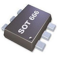
Package / Case
SOT-666
Collector- Emitter Voltage Vceo Max
- 50 V
Peak Dc Collector Current
- 100 mA
Power Dissipation
200 mW
Maximum Operating Temperature
+ 150 C
Emitter- Base Voltage Vebo
- 10 V
Minimum Operating Temperature
- 65 C
Power - Max
300mW
Current - Collector (ic) (max)
100mA
Voltage - Collector Emitter Breakdown (max)
50V
Transistor Type
2 PNP - Pre-Biased (Dual)
Current - Collector Cutoff (max)
1µA
Dc Current Gain (hfe) (min) @ Ic, Vce
100 @ 5mA, 5V
Vce Saturation (max) @ Ib, Ic
100mV @ 250µA, 5mA
Resistor - Base (r1) (ohms)
10K
Resistor - Emitter Base (r2) (ohms)
47K
Frequency - Transition
-
Mounting Type
Surface Mount
Lead Free Status / RoHS Status
Lead free / RoHS Compliant
Frequency - Transition
-
Lead Free Status / Rohs Status
Lead free / RoHS Compliant
Other names
934057047115 PEMB9 T/R
Available stocks
Company
Part Number
Manufacturer
Quantity
Price
Company:

Part Number:
PEMB9,115
Manufacturer:
NXP Semiconductors
Quantity:
13 200
Part Number:
PEMB9,115
Manufacturer:
NEXPERIA/安世
Quantity:
20 000


NXP Semiconductors
ORDERING INFORMATION
LIMITING VALUES
In accordance with the Absolute Maximum Rating System (IEC 60134).
Notes
1. Device mounted on an FR4 printed-circuit board, single-sided copper, standard footprint.
2. Reflow soldering is the only recommended soldering method.
2003 Oct 03
PEMB9
PUMB9
Per transistor
V
V
V
V
I
I
P
T
T
T
Per device
P
SYMBOL
O
CM
TYPE NUMBER
stg
j
amb
CBO
CEO
EBO
I
tot
tot
PNP/PNP resistor-equipped transistors;
R1 = 10 kΩ, R2 = 47 kΩ
collector-base voltage
collector-emitter voltage
emitter-base voltage
input voltage
output current (DC)
peak collector current
total power dissipation
storage temperature
junction temperature
operating ambient temperature
total power dissipation
positive
negative
SOT363
SOT666
SOT363
SOT666
−
−
PARAMETER
NAME
plastic surface mounted package; 6 leads
plastic surface mounted package; 6 leads
open emitter
open base
open collector
T
note 1
notes 1 and 2
T
note 1
notes 1 and 2
amb
amb
≤ 25 °C
≤ 25 °C
3
CONDITIONS
DESCRIPTION
PACKAGE
−
−
−
−
−
−
−
−
−
−65
−
−65
−
−
MIN.
PEMB9; PUMB9
−50
−50
−10
+6
−40
−100
−100
200
200
+150
150
+150
300
300
MAX.
Product data sheet
SOT666
SOT363
VERSION
V
V
V
V
V
mA
mA
mW
mW
°C
°C
°C
mW
mW
UNIT
Related parts for PEMB9,115
Image
Part Number
Description
Manufacturer
Datasheet
Request
R

Part Number:
Description:
TRANSISTOR,PNP/PNP W/RES,50V,SOT666
Manufacturer:
NXP Semiconductors
Datasheet:
Part Number:
Description:
Digital Transistors TRNS DOUBL RET TAPE7
Manufacturer:
NXP Semiconductors
Datasheet:

Part Number:
Description:
TRANSISTOR PNP/PNP RES SOT666
Manufacturer:
NXP Semiconductors
Datasheet:
Part Number:
Description:
NXP Semiconductors designed the LPC2420/2460 microcontroller around a 16-bit/32-bitARM7TDMI-S CPU core with real-time debug interfaces that include both JTAG andembedded trace
Manufacturer:
NXP Semiconductors
Datasheet:

Part Number:
Description:
NXP Semiconductors designed the LPC2458 microcontroller around a 16-bit/32-bitARM7TDMI-S CPU core with real-time debug interfaces that include both JTAG andembedded trace
Manufacturer:
NXP Semiconductors
Datasheet:
Part Number:
Description:
NXP Semiconductors designed the LPC2468 microcontroller around a 16-bit/32-bitARM7TDMI-S CPU core with real-time debug interfaces that include both JTAG andembedded trace
Manufacturer:
NXP Semiconductors
Datasheet:
Part Number:
Description:
NXP Semiconductors designed the LPC2470 microcontroller, powered by theARM7TDMI-S core, to be a highly integrated microcontroller for a wide range ofapplications that require advanced communications and high quality graphic displays
Manufacturer:
NXP Semiconductors
Datasheet:
Part Number:
Description:
NXP Semiconductors designed the LPC2478 microcontroller, powered by theARM7TDMI-S core, to be a highly integrated microcontroller for a wide range ofapplications that require advanced communications and high quality graphic displays
Manufacturer:
NXP Semiconductors
Datasheet:
Part Number:
Description:
The Philips Semiconductors XA (eXtended Architecture) family of 16-bit single-chip microcontrollers is powerful enough to easily handle the requirements of high performance embedded applications, yet inexpensive enough to compete in the market for hi
Manufacturer:
NXP Semiconductors
Datasheet:
Part Number:
Description:
The XA-S3 device is a member of Philips Semiconductors? XA(eXtended Architecture) family of high performance 16-bitsingle-chip microcontrollers
Manufacturer:
NXP Semiconductors
Datasheet:

Part Number:
Description:
The NXP BlueStreak LH75401/LH75411 family consists of two low-cost 16/32-bit System-on-Chip (SoC) devices
Manufacturer:
NXP Semiconductors
Datasheet:
Part Number:
Description:
The NXP LPC3130/3131 combine an 180 MHz ARM926EJ-S CPU core, high-speed USB2
Manufacturer:
NXP Semiconductors
Datasheet:
Part Number:
Description:
The NXP LPC3141 combine a 270 MHz ARM926EJ-S CPU core, High-speed USB 2
Manufacturer:
NXP Semiconductors
Part Number:
Description:
The NXP LPC3143 combine a 270 MHz ARM926EJ-S CPU core, High-speed USB 2
Manufacturer:
NXP Semiconductors