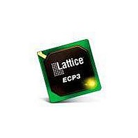
LFE3-150EA-7FN1156CTW Lattice, LFE3-150EA-7FN1156CTW Datasheet - Page 98

LFE3-150EA-7FN1156CTW
Manufacturer Part Number
LFE3-150EA-7FN1156CTW
Description
FPGA - Field Programmable Gate Array 149K LUTs 586 I/O 1.2V -7 Speed
Manufacturer
Lattice
Datasheet
1.LFE3-150EA-7FN672CTW.pdf
(130 pages)
Specifications of LFE3-150EA-7FN1156CTW
Number Of Programmable I/os
133 to 586
Data Ram Size
6.85 Mbits
Delay Time
37 ns
Supply Voltage (max)
1.26 V
Supply Current
18 mA
Maximum Operating Temperature
+ 85 C
Minimum Operating Temperature
0 C
Mounting Style
SMD/SMT
Supply Voltage (min)
1.14 V
Package / Case
FPBGA-1156
Lead Free Status / RoHS Status
Lead free / RoHS Compliant
Available stocks
Company
Part Number
Manufacturer
Quantity
Price
Company:
Part Number:
LFE3-150EA-7FN1156CTW
Manufacturer:
Lattice Semiconductor Corporation
Quantity:
10 000
- Current page: 98 of 130
- Download datasheet (3Mb)
Lattice Semiconductor
HDMI (High-Definition Multimedia Interface) Electrical and Timing
Characteristics
AC and DC Characteristics
Table 3-22. Transmit and Receive
Transmit
Intra-pair Skew
Inter-pair Skew
TMDS Differential Clock Jitter
Receive
R
V
TMDS Clock Jitter
1. Output buffers must drive a translation device. Max. speed is 2Gbps. If translation device does not modify rise/fall time, the maximum speed
2. Input buffers must be AC coupled in order to support the 3.3V common mode. Generally, HDMI inputs are terminated by an external cable
T
ICM
is 1.5Gbps.
equalizer before data/clock is forwarded to the LatticeECP3 device.
Symbol
Termination Resistance
Input AC Common Mode Voltage (50-ohm Setting)
Clock Jitter Tolerance
1, 2
Description
3-46
DC and Switching Characteristics
LatticeECP3 Family Data Sheet
Min. Spec.
Spec. Compliance
40
—
—
—
—
—
Max. Spec.
0.25
0.25
800
75
60
50
Ohms
Units
mV
ps
ps
UI
UI
Related parts for LFE3-150EA-7FN1156CTW
Image
Part Number
Description
Manufacturer
Datasheet
Request
R

Part Number:
Description:
FPGA - Field Programmable Gate Array 149K LUTs 380 I/O 1.2V -7 Speed
Manufacturer:
Lattice
Datasheet:

Part Number:
Description:
FPGA - Field Programmable Gate Array 149K LUTs 380 I/O 1.2V -7 SPEED
Manufacturer:
Lattice
Datasheet:

Part Number:
Description:
FPGA - Field Programmable Gate Array 149K LUTs 380 I/O 1.2V -7 SPEED
Manufacturer:
Lattice
Datasheet:

Part Number:
Description:
FPGA - Field Programmable Gate Array 149K LUTs 586 I/O 1.2V -7 SPEED
Manufacturer:
Lattice
Datasheet:

Part Number:
Description:
FPGA - Field Programmable Gate Array 149K LUTs 586 I/O 1.2V -7 SPEED
Manufacturer:
Lattice
Datasheet:

Part Number:
Description:
FPGA - Field Programmable Gate Array 149K LUTs 586 I/O 1.2V -7 Speed
Manufacturer:
Lattice

Part Number:
Description:
FPGA - Field Programmable Gate Array 149K LUTs 380 I/O 1.2V -7 Speed
Manufacturer:
Lattice
Part Number:
Description:
FPGA LatticeECP3™ Family 149000 Cells 65nm Technology 1.2V 672-Pin FBGA
Manufacturer:
LATTICE SEMICONDUCTOR
Datasheet:

Part Number:
Description:
IC FPGA 149KLUTS 380I/O 672FPBGA
Manufacturer:
Lattice
Datasheet:

Part Number:
Description:
IC FPGA 149KLUTS 586I/O 1156BGA
Manufacturer:
Lattice
Datasheet:

Part Number:
Description:
IC FPGA 149KLUTS 586I/O 1156BGA
Manufacturer:
Lattice
Datasheet:

Part Number:
Description:
IC FPGA 149KLUTS 380I/O 672-BGA
Manufacturer:
Lattice
Datasheet:

Part Number:
Description:
IC FPGA 149KLUTS 380I/O 672-BGA
Manufacturer:
Lattice
Datasheet:

Part Number:
Description:
IC FPGA 149KLUTS 586I/O 1156-BGA
Manufacturer:
Lattice
Datasheet:

Part Number:
Description:
IC FPGA 149KLUTS 380I/O 672-BGA
Manufacturer:
Lattice
Datasheet:


