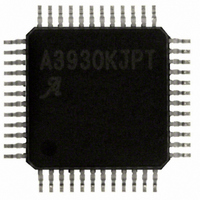
A3930KJPTR-T Allegro Microsystems Inc, A3930KJPTR-T Datasheet - Page 14

A3930KJPTR-T
Manufacturer Part Number
A3930KJPTR-T
Description
IC,Motor Controller,QFP,48PIN
Manufacturer
Allegro Microsystems Inc
Datasheet
1.A3930KJPTR-T.pdf
(21 pages)
Specifications of A3930KJPTR-T
Applications
DC Motor Controller, Brushless (BLDC), 3 Phase
Number Of Outputs
1
Current - Output
500mA
Voltage - Supply
5.5 V ~ 50 V
Operating Temperature
-40°C ~ 150°C
Mounting Type
Surface Mount
Package / Case
48-LFQFP Exposed Pad
Lead Free Status / RoHS Status
Lead free / RoHS Compliant
Voltage - Load
-
Lead Free Status / RoHS Status
Lead free / RoHS Compliant
Other names
620-1289-2
A3930KJPTR-T
A3930KJPTR-T
Available stocks
Company
Part Number
Manufacturer
Quantity
Price
Company:
Part Number:
A3930KJPTR-T
Manufacturer:
ALLEGRO
Quantity:
1 001
Company:
Part Number:
A3930KJPTR-T
Manufacturer:
Allegro MicroSystems, LLC
Quantity:
10 000
Part Number:
A3930KJPTR-T
Manufacturer:
ALLEGRO/雅丽高
Quantity:
20 000
A3930
A3931
Power
All supply connections to the A3930/A3931 should have capaci-
tors mounted between the supply pins and the ground pin. These
capacitors will provide the transient currents which occur during
switching and decouple any voltage transients on the pin from the
main supply.
VBB Decouple with at least a 100 nF ceramic capacitor mounted
between the VBB pin and the AGND pin. A larger electrolytic
capacitor, typically 10 μF, in parallel with the ceramic capacitor
is also recommended.
VREG Supplies current for the gate-drive circuit. As the gates
are driven high, they require current from an external capacitor
connected to VREG to support the transients. This capacitor
should be placed as close as possible to the VREG pin with the
ground connection close to the AGND pin. Its value should be at
least 20 times larger than the bootstrap capacitor. The capacitor
should have a very low series resistance (ESR) and inductance
(ESL) to avoid large voltage drops during the initial transient.
The optimum capacitor type is a high quality ceramic such as
X7R. However, when the required capacitance is too large, an
aluminium electrolytic capacitor may be used, with a smaller
ceramic capacitor (≈100 nF) in parallel.
V5 When the 5V regulator is used with an external pass transistor
to provide power to other circuits, a 10 μF decoupling capacitor
should be connected between the V5 pin and AGND as close to
the pins as possible. If an electrolytic capacitor is used, then a
100 nF ceramic capacitor should be added in parallel. To improve
stability, a 100 nF capacitor also should be connected between
the V5BD pin and AGND. If 5V is not required for external
circuits, the external pass transistor may be omitted, but in that
case, V5 must connected directly to V5BD and decoupled with at
least a 220 nF capacitor between V5 and AGND.
AGND The A3930/A3931 has a single ground connection at the
AGND pin. The design ensures that only the operating current
for the controller stage passes through this pin. The charge and
discharge current for the external FETs does not pass though this
pin. The AGND pin is the ground reference for the current trip
threshold, the V
It should therefor be kept as quiet as possible. A suggested ground
connection scheme is described in the layout section below.
and
DS
monitor threshold, and the timing components.
Applications Information
Automotive 3-Phase BLDC Controller
Power Dissipation In applications where a high ambient tem-
perature is expected the on-chip power dissipation may become
a critical factor. Careful attention should be paid to ensure the
operating conditions allow the A3930/A3931 to remain in a safe
range of junction temperature.
The power consumed, P
mated using the following formulas:
where I
where V
where V
where N = 2 for slow decay, or N = 4 for fast decay, and
Bootstrap Capacitors
Bootstrap Capacitor Selection The value for C
be correctly selected to ensure proper operation of the device. If
the value is too large, time will be wasted charging the capacitor,
resulting in a limit on the maximum duty cycle and PWM
frequency. If the value is too small, there can be a large voltage
drop at the time when the charge is transferred from C
MOSFET gate.
To keep the voltage drop small, Q
a reasonable value. To calculate C
can be used:
therefore
The voltage drop on the Cx pin as the MOSFET is being turned
on can be approximated by:
Bootstrap Charging It is good practice to ensure that the high-
side bootstrap capacitor, CBOOT, is completely charged before a
P
SWITCHING
P
P
BB
Q
C
BB
BB
CPUMP
CPUMP
P
Ratio = 10 / (R
P
BOOT
BOOT
BIAS
is 3 mA, typical, and
TOT
ΔV = Q
< 15 V, or
> 15 V, and
I
AV
= P
= V
= (2 × V
= (V
= Q
= Q
= C
= Q
= Q
BIAS
BB
BOOT
GATE
GATE
GATE
GATE
GATE
BB
× I
–V
BB
GATE
+ P
TOT
× N × f
× V
× 20,
× 20 / V
/ C
× V
and MOSFET Driver
BB
REG
–V
CPUMP
115 Northeast Cutoff
1.508.853.5000; www.allegromicro.com
BOOT
Allegro MicroSystems, Inc.
Worcester, Massachusetts 01615-0036 U.S.A.
,
, by the A3930/A3931 can be esti-
REG
BOOT
) × I
REG
+ 10)
PWM
× N × f
BOOT
) × I
AV
,
BOOT
BOOT
+ P
,
AV
SWITCHING
, the following formulas
Q
PWM
GATE
× Ratio
.
,
A factor of 20 is
BOOT
BOOT
must
to the
14


