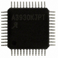
A3930KJPTR-T Allegro Microsystems Inc, A3930KJPTR-T Datasheet - Page 16

A3930KJPTR-T
Manufacturer Part Number
A3930KJPTR-T
Description
IC,Motor Controller,QFP,48PIN
Manufacturer
Allegro Microsystems Inc
Datasheet
1.A3930KJPTR-T.pdf
(21 pages)
Specifications of A3930KJPTR-T
Applications
DC Motor Controller, Brushless (BLDC), 3 Phase
Number Of Outputs
1
Current - Output
500mA
Voltage - Supply
5.5 V ~ 50 V
Operating Temperature
-40°C ~ 150°C
Mounting Type
Surface Mount
Package / Case
48-LFQFP Exposed Pad
Lead Free Status / RoHS Status
Lead free / RoHS Compliant
Voltage - Load
-
Lead Free Status / RoHS Status
Lead free / RoHS Compliant
Other names
620-1289-2
A3930KJPTR-T
A3930KJPTR-T
Available stocks
Company
Part Number
Manufacturer
Quantity
Price
Company:
Part Number:
A3930KJPTR-T
Manufacturer:
ALLEGRO
Quantity:
1 001
Company:
Part Number:
A3930KJPTR-T
Manufacturer:
Allegro MicroSystems, LLC
Quantity:
10 000
Part Number:
A3930KJPTR-T
Manufacturer:
ALLEGRO/雅丽高
Quantity:
20 000
A3930
A3931
Note that this blank time is only used to mask the internal cur-
rent comparator. If the current sense amplifier output, CSOUT,
is being used in an external PWM control circuit, then it will
be necessary to externally generate a blank time for that control
loop.
Dead Time The potential for cross-conduction occurs with
synchronous rectification, direction changes, PWM, or after a
bootstrap capacitor charging cycle. To prevent cross-conduction
in any phase of the power FET bridge, it is necessary to have a
dead-time delay, t
the next turn-on event. t
6.3 μs, and is set by the value of a resistor, RDEAD, between the
RDEAD pin and the GND pin. The maximum dead time of typi-
cally 6μs can be set by leaving the RDEAD pin unconnected, or
connected to the V5 pin.
At 25°C, the value of t
where I
greatest accuracy is obtained with values of R
10 and 100 kΩ.
The choice of power MOSFET and external series gate resistance
determines the selection of RDEAD. The dead time should be
made long enough to cover the variation of the MOSFET gate
capacitance and the tolerances of the series gate resistance, both
external and internal to the A3930/A3931.
Figure 2. Internal PWM RC Timing
RC
V
V
GHx
Current
Trip Points
GLx
RCH
RCL
+V
DEAD
0
t
I
DEAD(nom)
DEAD
is in μA, and
= 2000 / R
and
DEAD
≈ 0.1 + 33 / (5 + I
t
DEAD
DEAD
t
, between a high- or low-side turn-off and
RC
DEAD
R
DEAD
DEAD
t
(μs) can be approximated by:
OSC
is in the range of between 96 ns and
is between 5 and 400 kΩ. The
t
DEAD
DEAD
t
BLANK
),
Note: For reasons of
clarity, t
exaggerated.
DEAD
DEAD
between
is shown
Automotive 3-Phase BLDC Controller
Synchronous Rectification To reduce power dissipation in
the external MOSFETs, the A3930/A3931 control logic turns
on the appropriate low-side and high-side driver during the load
current recirculation PWM-off cycle. Synchronous rectification
allows current to flow through the FET selected by the MODE
pin setting during the decay time, rather than through the source-
drain body diode. The body diodes of the recirculating power
FETs conduct only during the dead time that occurs at each PWM
transition. For internal current control using fast decay mode,
reversal of load current is prevented by turning off synchronous
rectification when a zero current level is detected. For external
PWM control using fast decay mode, the load current will not be
limited to zero but will rise to the set current limit in the reverse
direction before disabling synchronous rectification.
Braking. The A3930 and A3931 provide dynamic braking by
forcing all low-side MOSFETs on, and all high-side MOSFETs
off. This effectively short-circuits the back EMF of the motor,
which forces a reverse current in the windings, and creating a
breaking torque.
During braking, the load current can be approximated by:
Because the load current does not flow through the sense resistor,
RSENSE, during a dynamic brake, care must be taken to ensure
that the power MOSFET maximum ratings are not exceeded.
It is possible to apply a PWM signal to the BRAKE input to
limit the motor braking current. However, because there is
no measurement of this current, the PWM duty cycle must be
determined for each set of conditions. Typically the duty cycle
of such a brake PWM input would start at a value which limits
the current and then drops to 0%, that is, BRAKE goes to low, to
hold the motor stationary.
Setting RESET = 1 and COAST = 0 overrides BRAKE and turns
all motor bridge FETs off, coasting the motor.
Driving a Full-Bridge. The A3930 and A3931 may be used
to drive a full-bridge (for example, a brush DC motor load) by
hard-wiring a single state for the Hall inputs and leaving the
corresponding phase driver outputs floating. For example, with a
configuration of H1 = H2 = 1, and H3 = 0, the outputs CC, GHC,
SC, and GLC would be floated, according to the commutation
truth table, table3, which indicates a state of high-impedence (Z)
for SC with that Hall input configuration. The DIR input
controls the motor rotation, while the PWM and MODE
inputs control the motor current behavior, as described in the
input logic table, table 3.
I
BRAKE
and MOSFET Driver
115 Northeast Cutoff
1.508.853.5000; www.allegromicro.com
Allegro MicroSystems, Inc.
Worcester, Massachusetts 01615-0036 U.S.A.
≈ V
BEMF
/ R
LOAD
16


