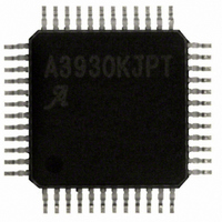
A3930KJPTR-T Allegro Microsystems Inc, A3930KJPTR-T Datasheet - Page 8

A3930KJPTR-T
Manufacturer Part Number
A3930KJPTR-T
Description
IC,Motor Controller,QFP,48PIN
Manufacturer
Allegro Microsystems Inc
Datasheet
1.A3930KJPTR-T.pdf
(21 pages)
Specifications of A3930KJPTR-T
Applications
DC Motor Controller, Brushless (BLDC), 3 Phase
Number Of Outputs
1
Current - Output
500mA
Voltage - Supply
5.5 V ~ 50 V
Operating Temperature
-40°C ~ 150°C
Mounting Type
Surface Mount
Package / Case
48-LFQFP Exposed Pad
Lead Free Status / RoHS Status
Lead free / RoHS Compliant
Voltage - Load
-
Lead Free Status / RoHS Status
Lead free / RoHS Compliant
Other names
620-1289-2
A3930KJPTR-T
A3930KJPTR-T
Available stocks
Company
Part Number
Manufacturer
Quantity
Price
Company:
Part Number:
A3930KJPTR-T
Manufacturer:
ALLEGRO
Quantity:
1 001
Company:
Part Number:
A3930KJPTR-T
Manufacturer:
Allegro MicroSystems, LLC
Quantity:
10 000
Part Number:
A3930KJPTR-T
Manufacturer:
ALLEGRO/雅丽高
Quantity:
20 000
A3930
A3931
Basic Operation
The A3930 and A3931 devices provide commutation and current
control for 3-phase brushless DC (BLDC) motors with integrated
Hall-effect (HE) sensors. The motor current is provided by an
external 3-phase N-channel MOSFET bridge which is controlled
by the A3930/A3931, using fixed-frequency pulse width modu-
lation (PWM). The use of PWM with N-channel MOSFETs
provides the most cost-effective solution for a high-efficiency
motor drive.
The A3930/A3931 provides all the necessary circuits to ensure
that the gate-source voltage of both high-side and low-side exter-
nal MOSFETs are above 10 V, at supply voltages down to 7 V.
For extreme battery voltage drop conditions, functional operation
is guaranteed down to 5.5 V but with a reduced gate drive. The
A3930/A3931 also decodes the commutation sequence from three
HE sensors spaced at 120° in the electrical cycle, and ensure no
cross-conduction (shoot through) in the external bridge. Individ-
ual pins provide direction, brake and coast control.
Motor current can be sensed by a low-value sense resistor,
RSENSE, in the ground connection to the bridge, amplified and
compared to a reference value. The A3930/A3931 then limits the
bridge current on a cycle-by-cycle basis. Bridge current can also
be controlled using an external PWM signal with the internal cur-
rent control either disabled or used to set the absolute maximum
motor current. Specific functions are described more fully in the
following sections.
Power Supplies
Only one power connection is required because all internal
circuits are powered by integrated regulators. The main power
supply should be connected to VBB through a reverse battery
protection circuit.
V5 and V5BD A 5 V supply for external pull-up and bias cur-
rents is provided by an integrated 5 V regulator controller and an
external NPN transistor, QV5. The A3930/A3931 provides the
base drive current on the V5BD pin, and the 5 V reference on the
V5 pin. This regulator is also used by the internal logic circuits
and must always be decoupled by at least a 200 nF capacitor,
CV5, between the V5 pin and AGND. For stability, a 100 nF
capacitor, C5BD, also should be connected between V5BD and
and
Functional Description
Automotive 3-Phase BLDC Controller
AGND. If an external 5 V supply is not required, the V5BD pin
and the V5 pin should be connected together.
CP1, CP2, and VREG The gate drive outputs are powered by
an internal charge pump, which requires a pump capacitor, typi-
cally 470 nF, CP, connected between the CP1 and CP2 pins. The
output from the charge pump, 13 V nominal, is used to power
each of the three high- and low-side driver pairs and is also
available on the VREG pin. A sufficiently large storage capaci-
tor, CREG, must be connected to this pin to provide the tran-
sient charging current to the low-side drivers. The charge pump
also provides the charging current for the bootstrap capacitors,
CBOOTx.
An additional “top-off” charge pump is provided for each high-
side drive which allows the high-side drive to maintain the gate
voltage on the external FET indefinitely, ensuring so-called 100%
PWM if required. This is a low-current trickle charge pump
(< 100 μA typical), and is only operated after a high-side driver
has been signaled to turn on. There is a small amount of bias
current (< 20 μA) drawn from the Cx pin to operate the floating
high-side circuit, and the charge pump simply provides enough
drive to ensure that the bootstrap voltage, and hence the gate volt-
age, will not droop due to this bias current. The charge required
for initial turn-on of the high-side gate is always supplied by
bootstrap capacitor charge cycles.
Hall Effect Sensor Inputs
H1, H2, and H3 Hall-effect sensor inputs are configured for
motors with 120° electrically-spaced HE sensors, but may be
used for 60° electrical spacing with an external inverter. HE sen-
sors usually require an additional pull-up resistor to be connected
between the sensor output and 5 V. This 5 V can be provided by
the integrated 5 V regulator. HE inputs have a hysteresis of typi-
cally 500 mV to reduce the effects of switching noise on the HE
connections to the motor. These inputs are also filtered to further
reduce the effects of switching noise. The HE inputs are pulled-
up to 5 V inside the A3930/A3931 through a high value (100
kΩ typical) resistor in series with a diode. This internal pull-up
makes the HE input appear high if the Hall sensor signal is miss-
ing, allowing detection of an HE input logic fault.
and MOSFET Driver
115 Northeast Cutoff
1.508.853.5000; www.allegromicro.com
Allegro MicroSystems, Inc.
Worcester, Massachusetts 01615-0036 U.S.A.
8


