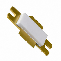
BLA0912-250,112 NXP Semiconductors, BLA0912-250,112 Datasheet - Page 3

BLA0912-250,112
Manufacturer Part Number
BLA0912-250,112
Description
TRANS LDMOS NCH 75V SOT502A
Manufacturer
NXP Semiconductors
Datasheet
1.BLA0912-250112.pdf
(13 pages)
Specifications of BLA0912-250,112
Transistor Type
LDMOS
Frequency
960MHz ~ 1.22GHz
Gain
13dB
Voltage - Rated
75V
Current Rating
1µA
Voltage - Test
36V
Power - Output
250W
Package / Case
SOT502A
Configuration
Single
Transistor Polarity
N-Channel
Resistance Drain-source Rds (on)
0.06 Ohms
Drain-source Breakdown Voltage
75 V
Gate-source Breakdown Voltage
+/- 22 V
Power Dissipation
700 W
Maximum Operating Temperature
+ 200 C
Mounting Style
SMD/SMT
Minimum Operating Temperature
- 65 C
Application
Avionics
Channel Type
N
Channel Mode
Enhancement
Drain Source Voltage (max)
75V
Output Power (max)
250W(Min)
Power Gain (typ)@vds
13@36VdB
Frequency (min)
960MHz
Frequency (max)
1.215GHz
Package Type
LDMOST
Pin Count
3
Forward Transconductance (typ)
9S
Drain Source Resistance (max)
60(Typ)@9Vmohm
Operating Temp Range
-65C to 200C
Drain Efficiency (typ)
50%
Mounting
Screw
Mode Of Operation
Class-AB
Number Of Elements
1
Power Dissipation (max)
700000mW
Vswr (max)
5
Screening Level
Military
Lead Free Status / RoHS Status
Lead free / RoHS Compliant
Noise Figure
-
Current - Test
-
Lead Free Status / Rohs Status
Details
Other names
934057490112
BLA0912-250
BLA0912-250
BLA0912-250
BLA0912-250
NXP Semiconductors
6. Characteristics
BLA0912-250
Product data sheet
6.1 Ruggedness in class-AB operation
Table 6.
T
Table 7.
RF performance in common source class-AB circuit; T
specified.
The BLA0912-250 is capable of withstanding a load mismatch corresponding to
VSWR = 5 : 1 through all phases under the following conditions: V
f = 960 MHz to 1215 MHz at rated load power.
Symbol Parameter
V
V
I
I
I
g
R
Symbol
V
f
P
G
η
Z
T
P
α
t
t
DSS
DSX
GSS
r
f
j
fs
D
th(j-h)
h
resp(sp)
(BR)DSS
GS(th)
DS
L
droop(pulse)
DS(on)
p
= 25
°
C; per section unless otherwise specified.
drain-source breakdown voltage V
gate-source threshold voltage
drain leakage current
drain cut-off current
gate leakage current
forward transconductance
drain-source on-state resistance V
DC characteristics
RF characteristics
Parameter
drain-source voltage
frequency
output power
power gain
drain efficiency
transient thermal impedance
from junction to heatsink
heatsink temperature
pulse droop power
spurious response
rise time
fall time
All information provided in this document is subject to legal disclaimers.
Rev. 3 — 26 November 2010
Conditions
V
V
V
V
V
V
Conditions
t
P
t
t
t
VSWR
GS
DS
GS
GS
DS
GS
DS
GS
p
p
p
p
L
= 100 μs; δ = 10 %
= 100 μs; δ = 10 %
= 100 μs; δ = 10 %
= 100 μs; δ = 10 %
= 250 W
= 10 V; I
= 10 V
= 10 V; I
= 0 V; I
= 0 V; V
= V
= 20 V; V
= 9 V; I
load
GSth
h
= 25
D
D
= 2 : 1
+ 9 V;
DS
D
D
= 3 mA
= 10 A
DS
= 300 mA
= 10 A
= 36 V
°
C; Z
= 0 V
th
Avionics LDMOS transistor
BLA0912-250
= 0.15 K/W; unless otherwise
Min
-
960
250
12
40
-
−55
-
-
-
-
Min
75
4
-
45
-
-
-
DS
= 36 V;
Typ
-
-
-
13
50
-
-
0.1
-
25
6
© NXP B.V. 2010. All rights reserved.
Typ
-
-
-
-
-
9
60
Max
36
1215
0.2
+70
0.5
−60
50
25
Max Unit
-
5
1
-
1
-
-
Unit
V
MHz
W
dB
%
K/W
°C
dB
dBc
ns
ns
3 of 13
V
V
μA
A
μA
S
mΩ


