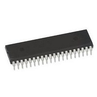
P80C31SBPN NXP Semiconductors, P80C31SBPN Datasheet - Page 22

P80C31SBPN
Manufacturer Part Number
P80C31SBPN
Description
MCU 8-Bit 80C 80C51 CISC ROMLess 3.3V/5V 40-Pin PDIP Tube
Manufacturer
NXP Semiconductors
Specifications of P80C31SBPN
Package
40PDIP
Device Core
80C51
Family Name
80C
Maximum Speed
16 MHz
Operating Supply Voltage
3.3|5 V
Data Bus Width
8 Bit
Number Of Programmable I/os
32
Interface Type
UART
Number Of Timers
3
Ram Size
128 Byte
Program Memory Type
ROMLess
Operating Temperature
0 to 70 °C
Controller Family/series
80C51
No. Of I/o's
32
Ram Memory Size
128Byte
Cpu Speed
16MHz
No. Of Timers
3
Digital Ic Case Style
DIP
Supply Voltage Range
2.7V To 5.5V
Core Size
8 Bit
Embedded Interface Type
UART
Rohs Compliant
Yes
Lead Free Status / RoHS Status
Lead free / RoHS Compliant
Available stocks
Company
Part Number
Manufacturer
Quantity
Price
Company:
Part Number:
P80C31SBPN
Manufacturer:
TDK-EPCOS
Quantity:
30 000
Company:
Part Number:
P80C31SBPN
Manufacturer:
PHILIPS
Quantity:
6
Part Number:
P80C31SBPN
Manufacturer:
PHILIPS/飞利浦
Quantity:
20 000
Company:
Part Number:
P80C31SBPNЈ¬112
Manufacturer:
NXP
Quantity:
7 020
Philips Semiconductors
DC ELECTRICAL CHARACTERISTICS
T
NOTES:
1. Typical ratings are not guaranteed. The values listed are at room temperature, 5 V.
2. Capacitive loading on ports 0 and 2 may cause spurious noise to be superimposed on the V
3. Capacitive loading on ports 0 and 2 may cause the V
4. Pins of ports 1, 2 and 3 source a transition current when they are being externally driven from 1 to 0. The transition current reaches its
5. See Figures 22 through 25 for I
6. This value applies to T
7. Load capacitance for port 0, ALE, and PSEN = 100 pF, load capacitance for all other outputs = 80 pF.
8. Under steady state (non-transient) conditions, I
9. ALE is tested to V
10. Pin capacitance is characterized but not tested. Pin capacitance is less than 25 pF. Pin capacitance of ceramic package is less than 15 pF
2000 Aug 07
amb
SYMBOL
SYMBOL
V
V
V
V
V
V
V
I
I
I
I
R
C
IL
TL
LI
CC
IL
IH
IH1
OL
OL1
OH
OH1
80C51 8-bit microcontroller family
128/256 byte RAM ROMless low voltage (2.7V–5.5V),
low power, high speed (33 MHz)
RST
IO
to external bus capacitance discharging into the port 0 and port 2 pins when these pins make 1-to-0 transitions during bus operations. In the
worst cases (capacitive loading > 100 pF), the noise pulse on the ALE pin may exceed 0.8 V. In such cases, it may be desirable to qualify
ALE with a Schmitt Trigger, or use an address latch with a Schmitt Trigger STROBE input. I
single output sinks more than 5mA and no more than two outputs exceed the test conditions.
address bits are stabilizing.
maximum value when V
If I
test conditions.
(except EA is 25 pF).
= 0 C to +70 C or –40 C to +85 C, 33 MHz devices; 5 V 10%; V
OL
Active mode:
Idle mode:
Maximum I
Maximum I
Maximum total I
exceeds the test condition, V
Input low voltage
Input high voltage (ports 0, 1, 2, 3, EA)
Input high voltage, XTAL1, RST
Output low voltage, ports 1, 2, 3
Output low voltage, port 0, ALE, PSEN
Output high voltage, ports 1, 2, 3
Output high voltage (port 0 in external bus
mode), ALE
Logical 0 input current, ports 1, 2, 3
Logical 1-to-0 transition current, ports 1, 2, 3
Input leakage current, port 0
Power supply current (see Figure 21):
Internal reset pull-down resistor
Pin capacitance
Active mode (see Note 5)
Idle mode (see Note 5)
Power-down mode or clock stopped (see Fig-
OL
OL
ure 25 for conditions)
per port pin:
per 8-bit port:
OH1
25 f
OL
I
I
CC(MAX)
CC(MAX)
9
, except when ALE is off then V
amb
for all outputs:
, PSEN
IN
PARAMETER
PARAMETER
10
is approximately 2 V.
= 0 C to +70 C. For T
(except EA)
diti
= 0.9
= 0.18
3
CC
test conditions.
OL
)
FREQ. + 1.1 mA
may exceed the related specification. Pins are not guaranteed to sink current greater than the listed
FREQ. +1.0 mA; See Figure 21.
15 mA (*NOTE: This is 85 C specification.)
26 mA
71 mA
8
3
OL
amb
7, 8
must be externally limited as follows:
= –40 C to +85 C, I
OH
OH
6
on ALE and PSEN to momentarily fall below the V
is the voltage specification.
T
0.45 < V
amb
4.5 V < V
T
amb
CONDITIONS
I
I
I
I
OH
= –40 C to +85 C
V
OL
V
OL
V
V
OH
V
V
See note 4
See note 5
CC
CC
CC
CC
= 0 C to 70 C
IN
IN
SS
22
TEST
= 1.6mA
= 3.2mA
= –3.2mA
IN
= –30 A
= 0.4 V
= 2.0 V
= 4.5 V
= 4.5 V
= 4.5 V
= 4.5 V
CC
< V
= 0 V
TL
< 5.5 V
CC
= –750 A.
2
2
– 0.3
0.2 V
V
V
0.7 V
CC
CC
OL
–0.5
MIN
OL
–1
40
CC
– 0.7
– 0.7
s of ALE and ports 1 and 3. The noise is due
can exceed these conditions provided that no
CC
+0.9
LIMITS
TYP
CC
3
1
–0.7 specification when the
80C31/80C32
0.2 V
V
V
CC
CC
MAX
–650
–50
225
0.4
0.4
Product specification
50
75
15
CC
10
+0.5
+0.5
–0.1
UNIT
UNIT
k
pF
V
V
V
V
V
V
V
A
A
A
A
A


