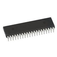
P80C31SBPN NXP Semiconductors, P80C31SBPN Datasheet - Page 25

P80C31SBPN
Manufacturer Part Number
P80C31SBPN
Description
MCU 8-Bit 80C 80C51 CISC ROMLess 3.3V/5V 40-Pin PDIP Tube
Manufacturer
NXP Semiconductors
Specifications of P80C31SBPN
Package
40PDIP
Device Core
80C51
Family Name
80C
Maximum Speed
16 MHz
Operating Supply Voltage
3.3|5 V
Data Bus Width
8 Bit
Number Of Programmable I/os
32
Interface Type
UART
Number Of Timers
3
Ram Size
128 Byte
Program Memory Type
ROMLess
Operating Temperature
0 to 70 °C
Controller Family/series
80C51
No. Of I/o's
32
Ram Memory Size
128Byte
Cpu Speed
16MHz
No. Of Timers
3
Digital Ic Case Style
DIP
Supply Voltage Range
2.7V To 5.5V
Core Size
8 Bit
Embedded Interface Type
UART
Rohs Compliant
Yes
Lead Free Status / RoHS Status
Lead free / RoHS Compliant
Available stocks
Company
Part Number
Manufacturer
Quantity
Price
Company:
Part Number:
P80C31SBPN
Manufacturer:
TDK-EPCOS
Quantity:
30 000
Company:
Part Number:
P80C31SBPN
Manufacturer:
PHILIPS
Quantity:
6
Part Number:
P80C31SBPN
Manufacturer:
PHILIPS/飞利浦
Quantity:
20 000
Company:
Part Number:
P80C31SBPNЈ¬112
Manufacturer:
NXP
Quantity:
7 020
Philips Semiconductors
EXPLANATION OF THE AC SYMBOLS
Each timing symbol has five characters. The first character is always
‘t’ (= time). The other characters, depending on their positions,
indicate the name of a signal or the logical status of that signal. The
designations are:
A – Address
C – Clock
D – Input data
H – Logic level high
I – Instruction (program memory contents)
L – Logic level low, or ALE
2000 Aug 07
PORT 0
PORT 2
80C51 8-bit microcontroller family
128/256 byte RAM ROMless low voltage (2.7V–5.5V),
low power, high speed (33 MHz)
PSEN
ALE
RD
PORT 0
PORT 2
PSEN
ALE
t
AVLL
FROM RI OR DPL
A0–A7
t
LLAX
t
t
AVWL
LHLL
t
t
LLWL
AVLL
A0–A7
Figure 14. External Program Memory Read Cycle
t
t
AVDV
P2.0–P2.7 OR A8–A15 FROM DPF
RLAZ
Figure 15. External Data Memory Read Cycle
t
LLDV
t
t
t
AVIV
LLAX
LLPL
t
LLIV
t
t
PLIV
RLDV
A0–A15
t
PLAZ
t
PLPH
t
RLRH
t
PXIX
INSTR IN
25
t
RHDX
DATA IN
P – PSEN
Q – Output data
R – RD signal
t – Time
V – Valid
W – WR signal
X – No longer a valid logic level
Z – Float
Examples: t
t
PXIZ
t
RHDZ
t
t
AVLL
WHLH
LLPL
= Time for address valid to ALE low.
=Time for ALE low to PSEN low.
A0–A7
A0–A7 FROM PCL
A0–A15 FROM PCH
A8–A15
80C31/80C32
Product specification
SU00006
INSTR IN
SU00025


