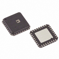
AD9514BCPZ Analog Devices Inc, AD9514BCPZ Datasheet - Page 14

AD9514BCPZ
Manufacturer Part Number
AD9514BCPZ
Description
IC CLOCK DIST 3OUT PLL 32LFCSP
Manufacturer
Analog Devices Inc
Type
Fanout Buffer (Distribution), Dividerr
Datasheet
1.AD9514BCPZ-REEL7.pdf
(28 pages)
Specifications of AD9514BCPZ
Number Of Circuits
1
Ratio - Input:output
1:3
Differential - Input:output
Yes/Yes
Input
Differential
Output
CMOS, LVDS, LVPECL
Frequency - Max
1.6GHz
Voltage - Supply
3.135 V ~ 3.465 V
Operating Temperature
-40°C ~ 85°C
Mounting Type
Surface Mount
Package / Case
32-LFCSP
Frequency-max
1.6GHz
No. Of Multipliers / Dividers
3
No. Of Amplifiers
4
Supply Voltage Range
3.135V To 3.465V
Slew Rate
1V/ns
Operating Temperature Range
-40°C To +85°C
Digital Ic Case Style
LFCSP
Lead Free Status / RoHS Status
Lead free / RoHS Compliant
For Use With
AD9514/PCBZ - BOARD EVAL CLOCK 3CH AD9514
Lead Free Status / RoHS Status
Lead free / RoHS Compliant, Lead free / RoHS Compliant
Available stocks
Company
Part Number
Manufacturer
Quantity
Price
Company:
Part Number:
AD9514BCPZ
Manufacturer:
ADI
Quantity:
526
AD9514
TERMINOLOGY
Phase Jitter and Phase Noise
An ideal sine wave can be thought of as having a continuous
and even progression of phase with time from 0 to 360 degrees
for each cycle. Actual signals, however, display a certain amount
of variation from ideal phase progression over time. This
phenomenon is called phase jitter. Although there are many
causes that can contribute to phase jitter, one major component
is due to random noise that is characterized statistically as being
Gaussian (normal) in distribution.
This phase jitter leads to a spreading out of the energy of the
sine wave in the frequency domain, producing a continuous
power spectrum. This power spectrum is usually reported as a
series of values whose units are dBc/Hz at a given offset in
frequency from the sine wave (carrier). The value is a ratio
(expressed in dB) of the power contained within a 1 Hz
bandwidth with respect to the power at the carrier frequency.
For each measurement, the offset from the carrier frequency is
also given.
It is also meaningful to integrate the total power contained
within some interval of offset frequencies (for example, 10 kHz
to 10 MHz). This is called the integrated phase noise over that
frequency offset interval and can be readily related to the time
jitter due to the phase noise within that offset frequency
interval.
Phase noise has a detrimental effect on the performance of
ADCs, DACs, and RF mixers. It lowers the achievable dynamic
range of the converters and mixers, although they are affected
in somewhat different ways.
Rev. 0 | Page 14 of 28
Time Jitter
Phase noise is a frequency domain phenomenon. In the
time domain, the same effect is exhibited as time jitter. When
observing a sine wave, the time of successive zero crossings is
seen to vary. For a square wave, the time jitter is seen as a
displacement of the edges from their ideal (regular) times of
occurrence. In both cases, the variations in timing from the
ideal are the time jitter. Since these variations are random in
nature, the time jitter is specified in units of seconds root mean
square (rms) or 1 sigma of the Gaussian distribution.
Time jitter that occurs on a sampling clock for a DAC or an
ADC decreases the SNR and dynamic range of the converter.
A sampling clock with the lowest possible jitter provides the
highest performance from a given converter.
Additive Phase Noise
It is the amount of phase noise that is attributable to the device
or subsystem being measured. The phase noise of any external
oscillators or clock sources has been subtracted. This makes it
possible to predict the degree to which the device affects the
total system phase noise when used in conjunction with the
various oscillators and clock sources, each of which contribute
their own phase noise to the total. In many cases, the phase
noise of one element dominates the system phase noise.
Additive Time Jitter
It is the amount of time jitter that is attributable to the device
or subsystem being measured. The time jitter of any external
oscillators or clock sources has been subtracted. This makes it
possible to predict the degree to which the device will affect the
total system time jitter when used in conjunction with the
various oscillators and clock sources, each of which contribute
their own time jitter to the total. In many cases, the time jitter of
the external oscillators and clock sources dominates the system
time jitter.


