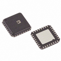
AD9514BCPZ Analog Devices Inc, AD9514BCPZ Datasheet - Page 25

AD9514BCPZ
Manufacturer Part Number
AD9514BCPZ
Description
IC CLOCK DIST 3OUT PLL 32LFCSP
Manufacturer
Analog Devices Inc
Type
Fanout Buffer (Distribution), Dividerr
Datasheet
1.AD9514BCPZ-REEL7.pdf
(28 pages)
Specifications of AD9514BCPZ
Number Of Circuits
1
Ratio - Input:output
1:3
Differential - Input:output
Yes/Yes
Input
Differential
Output
CMOS, LVDS, LVPECL
Frequency - Max
1.6GHz
Voltage - Supply
3.135 V ~ 3.465 V
Operating Temperature
-40°C ~ 85°C
Mounting Type
Surface Mount
Package / Case
32-LFCSP
Frequency-max
1.6GHz
No. Of Multipliers / Dividers
3
No. Of Amplifiers
4
Supply Voltage Range
3.135V To 3.465V
Slew Rate
1V/ns
Operating Temperature Range
-40°C To +85°C
Digital Ic Case Style
LFCSP
Lead Free Status / RoHS Status
Lead free / RoHS Compliant
For Use With
AD9514/PCBZ - BOARD EVAL CLOCK 3CH AD9514
Lead Free Status / RoHS Status
Lead free / RoHS Compliant, Lead free / RoHS Compliant
Available stocks
Company
Part Number
Manufacturer
Quantity
Price
Company:
Part Number:
AD9514BCPZ
Manufacturer:
ADI
Quantity:
526
APPLICATIONS
USING THE AD9514 OUTPUTS FOR ADC CLOCK
APPLICATIONS
Any high speed, analog-to-digital converter (ADC) is extremely
sensitive to the quality of the sampling clock provided by the
user. An ADC can be thought of as a sampling mixer, and any
noise, distortion, or timing jitter on the clock is combined with
the desired signal at the A/D output. Clock integrity require-
ments scale with the analog input frequency and resolution,
with higher analog input frequency applications at ≥14-bit
resolution being the most stringent. The theoretical SNR of an
ADC is limited by the ADC resolution and the jitter on the
sampling clock. Considering an ideal ADC of infinite resolution
where the step size and quantization error can be ignored, the
available SNR can be expressed approximately by
where f
T
Figure 35 shows the required sampling clock jitter as a function
of the analog frequency and effective number of bits (ENOB).
See Application Notes AN-756 and AN-501 at www.analog.com.
j
is the rms jitter on the sampling clock.
SNR
110
100
90
80
70
60
50
40
30
A
10
is the highest analog frequency being digitized.
Figure 35. ENOB and SNR vs. Analog Input Frequency
=
f
A
20
FULL-SCALE SINE WAVE ANALOG FREQUENCY (MHz)
×
log
⎡
⎢
⎢
⎣
2π
f
1
A
T
J
⎤
⎥
⎥
⎦
100
SNR = 20log
2πf
1
A
T
J
1k
18
16
14
12
10
8
6
Rev. 0 | Page 25 of 28
Many high performance ADCs feature differential clock inputs
to simplify the task of providing the required low jitter clock on
a noisy PCB. (Distributing a single-ended clock on a noisy PCB
can result in coupled noise on the sample clock. Differential
distribution has inherent common-mode rejection that can
provide superior clock performance in a noisy environment.)
The AD9514 features both LVPECL and LVDS outputs that
provide differential clock outputs, which enable clock solutions
that maximize converter SNR performance. The input
requirements of the ADC (differential or single-ended, logic
level, termination) should be considered when selecting the best
clocking/converter solution.
LVPECL CLOCK DISTRIBUTION
The low voltage, positive emitter-coupled, logic (LVPECL)
outputs of the AD9514 provide the lowest jitter clock signals
available from the AD9514. The LVPECL outputs (because they
are open emitter) require a dc termination to bias the output
transistors. The simplified equivalent circuit in Figure 31 shows
the LVPECL output stage.
In most applications, a standard LVPECL far-end termination is
recommended, as shown in Figure 36. The resistor network is
designed to match the transmission line impedance (50 Ω) and
the switching threshold (V
LVPECL
V
S
LVPECL
V
S
200Ω
Figure 37. LVPECL with Parallel Transmission Line
Figure 36. LVPECL Far-End Termination
V
(NOT COUPLED)
0.1nF
0.1nF
SINGLE-ENDED
T
200Ω
= V
S
100Ω DIFFERENTIAL
50Ω
50Ω
– 1.3V
S
− 1.3 V).
(COUPLED)
127Ω
83Ω
V
S
100Ω
127Ω
83Ω
LVPECL
AD9514
V
S
LVPECL
V
S


