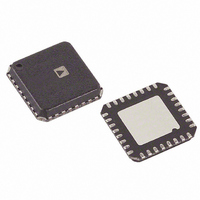
AD9514BCPZ Analog Devices Inc, AD9514BCPZ Datasheet - Page 3

AD9514BCPZ
Manufacturer Part Number
AD9514BCPZ
Description
IC CLOCK DIST 3OUT PLL 32LFCSP
Manufacturer
Analog Devices Inc
Type
Fanout Buffer (Distribution), Dividerr
Datasheet
1.AD9514BCPZ-REEL7.pdf
(28 pages)
Specifications of AD9514BCPZ
Number Of Circuits
1
Ratio - Input:output
1:3
Differential - Input:output
Yes/Yes
Input
Differential
Output
CMOS, LVDS, LVPECL
Frequency - Max
1.6GHz
Voltage - Supply
3.135 V ~ 3.465 V
Operating Temperature
-40°C ~ 85°C
Mounting Type
Surface Mount
Package / Case
32-LFCSP
Frequency-max
1.6GHz
No. Of Multipliers / Dividers
3
No. Of Amplifiers
4
Supply Voltage Range
3.135V To 3.465V
Slew Rate
1V/ns
Operating Temperature Range
-40°C To +85°C
Digital Ic Case Style
LFCSP
Lead Free Status / RoHS Status
Lead free / RoHS Compliant
For Use With
AD9514/PCBZ - BOARD EVAL CLOCK 3CH AD9514
Lead Free Status / RoHS Status
Lead free / RoHS Compliant, Lead free / RoHS Compliant
Available stocks
Company
Part Number
Manufacturer
Quantity
Price
Company:
Part Number:
AD9514BCPZ
Manufacturer:
ADI
Quantity:
526
SPECIFICATIONS
Typical (typ) is given for V
and maximum (max) values are given over full V
CLOCK INPUT
Table 1.
Parameter
CLOCK INPUT (CLK)
1
CLOCK OUTPUTS
Table 2.
Parameter
LVPECL CLOCK OUTPUTS
LVDS CLOCK OUTPUT
CMOS CLOCK OUTPUT
A slew rate of 1 V/ns is required to meet jitter, phase noise, and propagation delay specifications.
Input Frequency
Input Sensitivity
Input Common-Mode Voltage, V
Input Common-Mode Range, V
Input Sensitivity, Single-Ended
Input Resistance
Input Capacitance
(OUT0, OUT1) Differential
Output Frequency
Output High Voltage (V
Output Low Voltage (V
Output Differential Voltage (V
(OUT2) Differential
Output Frequency
Differential Output Voltage (V
Delta V
Output Offset Voltage (V
Delta V
Short-Circuit Current (I
(OUT2) Single-Ended
Output Frequency
Output Voltage High (V
Output Voltage Low (V
OD
OS
1
1
SA
OL
OL
OH
OH
, I
)
)
OS
)
)
SB
S
)
= 3.3 V ± 5%, T
)
OD
OD
CMR
)
)
CM
Min
0
V
V
640
0
250
1.125
0
V
S
S
S
− 1.1
− 1.90
− 0.1
A
Min
0
1.5
1.3
4.0
= 25°C, R
S
and T
Typ
V
V
790
350
1.23
14
Typ
150
1.6
150
4.8
2
S
S
− 0.96
− 1.76
SET
A
(−40°C to +85°C) variation.
= 4.12 kΩ, LVPECL V
Max
1.6
1.7
1.8
5.6
Rev. 0 | Page 3 of 28
Max
1.6
V
V
960
800
450
30
1.375
25
24
250
0.1
S
S
− 0.82
− 1.52
Unit
GHz
mV p-p
V
V
mV p-p
kΩ
pF
Unit
GHz
V
V
mV
MHz
mV
mV
V
mV
mA
MHz
V
V
OD
Test Conditions/Comments
Self-biased; enables ac coupling
With 200 mV p-p signal applied; dc-coupled
CLK ac-coupled; CLKB ac-bypassed to RF ground
Self-biased
= 790 mV, unless otherwise noted. Minimum (min)
Test Conditions/Comments
Termination = 50 Ω to V
Termination = 100 Ω differential
Output shorted to GND
Single-ended measurements; termination open
Complementary output on (OUT2B)
With 5 pF load
@ 1 mA load
@ 1 mA load
S
− 2 V
AD9514


